MONOS type nonvolatile memory cell, nonvolatile memory, and manufacturing method thereof

a nonvolatile memory, monos type technology, applied in the direction of basic electric elements, electrical equipment, semiconductor devices, etc., can solve the problems of insufficient film thickness in order, inability to realize the miniaturization of memory cells, and inability to reduce electric power consumption

Inactive Publication Date: 2007-08-30
KK TOSHIBA
View PDF7 Cites 48 Cited by
  • Summary
  • Abstract
  • Description
  • Claims
  • Application Information

AI Technical Summary

Benefits of technology

[0012] According to a first aspect of the present invention, there is provided a MONOS type nonvolatile memory cell comprising: a semiconductor substrate having a convex curved surface portion; a laminated insulating film which is formed of a tunnel insulating layer with a thickness of 4 to 10 nm, a charge storage insulating la...

Problems solved by technology

In order to make a direct tunneling current flow in the tunnel oxide film, in a quintessential way, it is necessary to apply a high voltage of about 10 to 20 V. Therefore, it is impossible to reduce electric power consumption.
Further, due to the need of insuring a desired withstand voltage among memory cells, it is impossible to realize the miniaturization of memory cells.
Such a film thickness is not sufficient in order to prevent an electric charge from escaping due to a self electric field at the time of data-retention.
Accordingly, when the memory cell is left for a long period after data writing, a quantity of stored electric charge is varied by escape of electric charge,...

Method used


Image

  • MONOS type nonvolatile memory cell, nonvolatile memory, and manufacturing method thereof
  • MONOS type nonvolatile memory cell, nonvolatile memory, and manufacturing method thereof
  • MONOS type nonvolatile memory cell, nonvolatile memory, and manufacturing method thereof

Examples


first embodiment

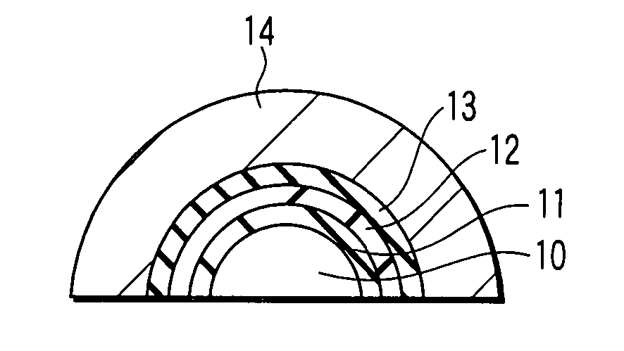
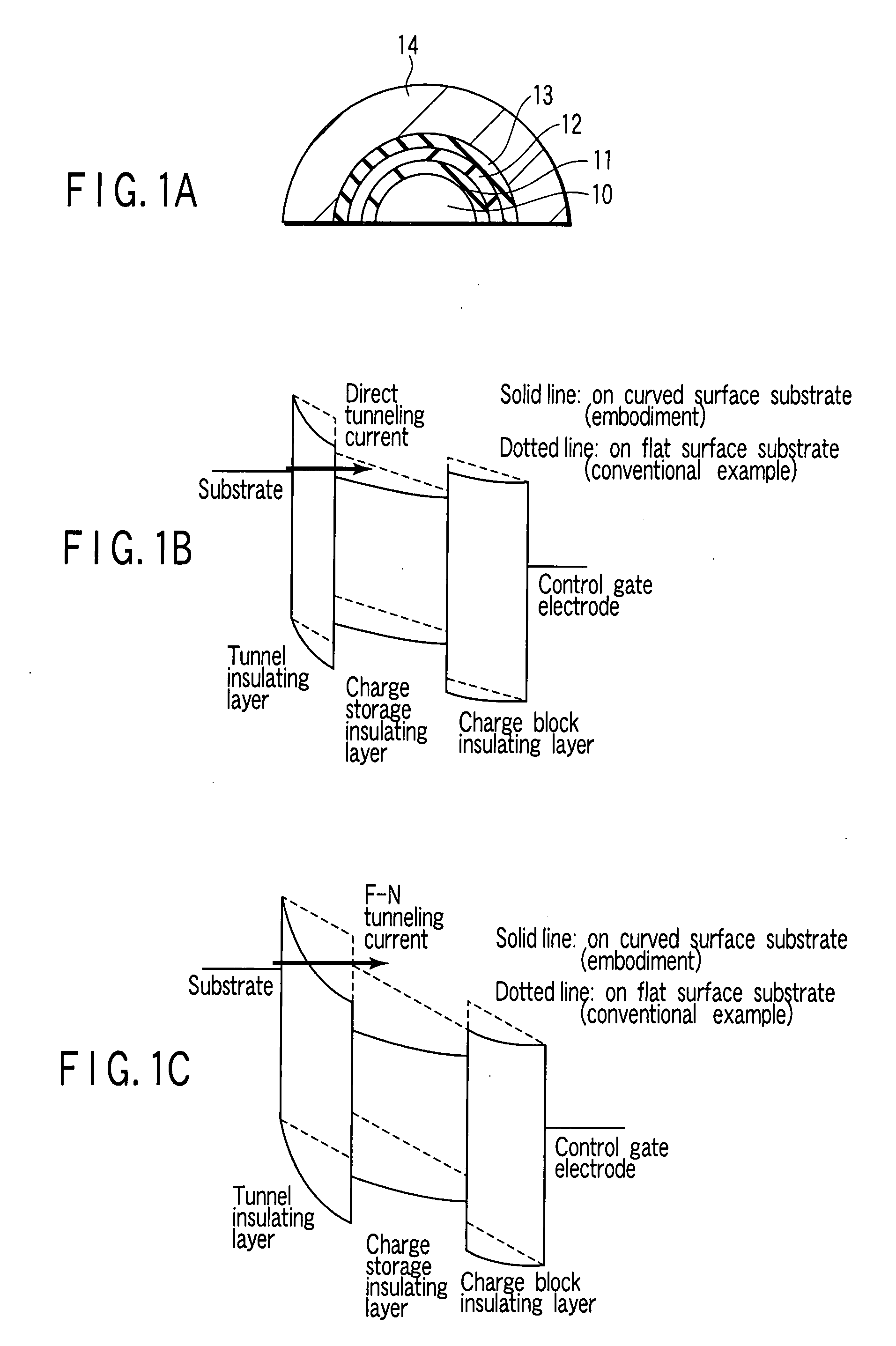
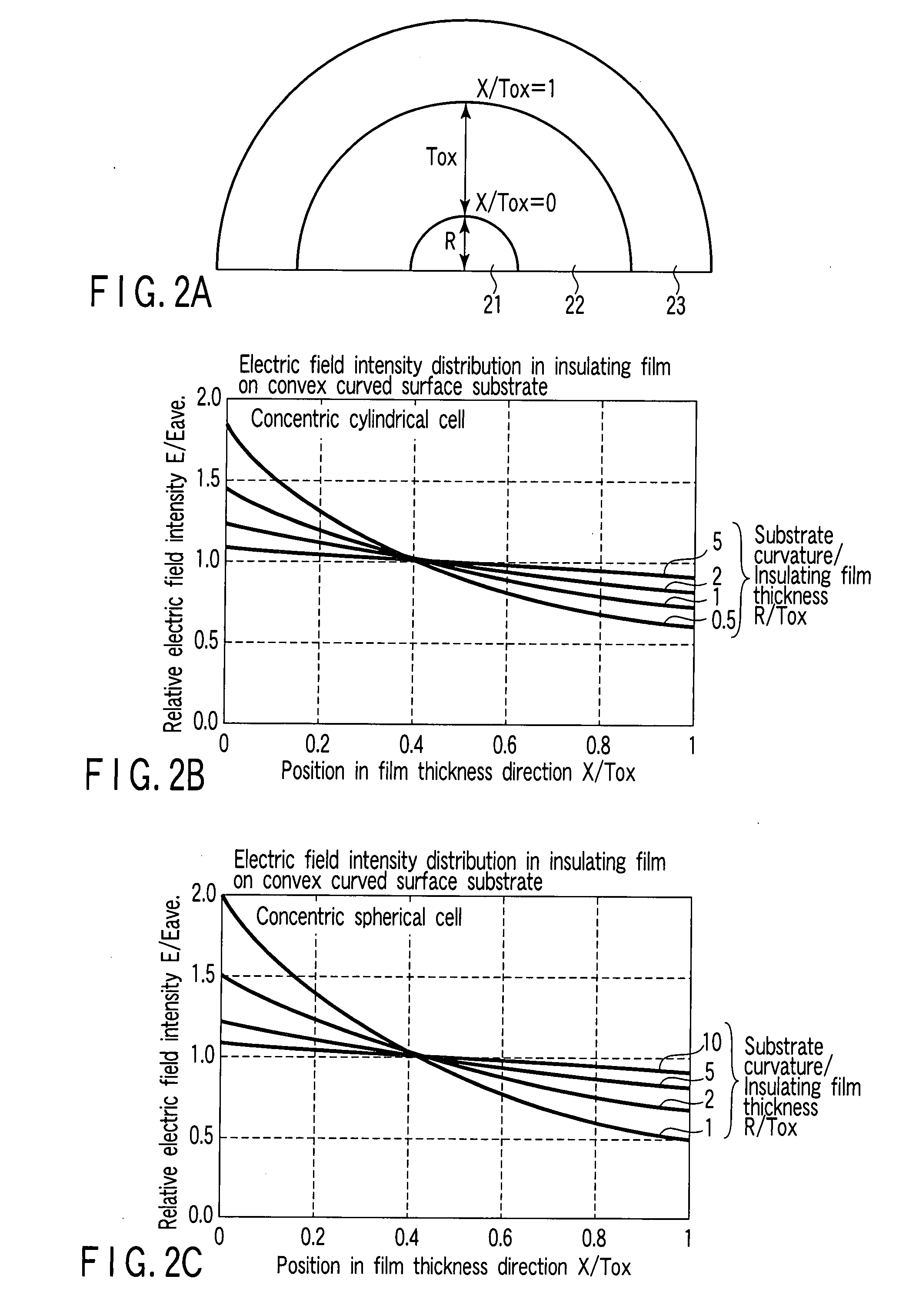
[0060]FIG. 4 shows a cross-sectional structure in a channel width direction (in a word line direction) of a memory cell in a MONOS nonvolatile memory having an array of a concentric cylindrical MONOS type memory cell according to a first embodiment.

[0061] In this memory cell, an isolation insulating film 41 formed of a silicon oxide film or the like is selectively provided on the surface of a semiconductor substrate 10 formed from semiconductor silicon or the like, and element regions sandwiched by the isolation insulating film 41 are projected to be convex curved surface portions 10a. Then, a charge storage insulating layer 12 formed of a silicon nitride film or the like is provided so as to sandwich a tunnel insulating layer 11 formed of a silicon oxide film or the like on the convex curved surface portions 10a of the substrate. In the present example, the substrate surface of portions facing the charge storage insulating layer 12 has convex curved surfaces in section in one dire...

second embodiment

[0089]FIG. 7A shows a cross-sectional structure in a channel width direction (in a word line direction) of the memory cell in the MONOS type nonvolatile memory having an array of concentric spherical MONOS type memory cells according to a second embodiment. FIG. 7B shows a cross-sectional structure in a channel length direction (in a bit line direction) of the memory cell of FIG. 7A.

[0090] In this memory cell, an isolation insulating films 41 formed of a silicon oxide film or the like are provided in parallel on the surface of a semiconductor substrate 10 formed of semiconductor silicon or the like, and element regions sandwiched by the isolation insulating films 41 are projected to be convex curved surface portions 10a. In the present example, the substrate surface of the portion facing a charge storage insulating layer formed in the following process has convex curved surfaces in sections in two directions perpendicular to one another. Moreover, diffusion layers (drain / source reg...


PUM


Abstract

A MONOS type nonvolatile memory cell is structured such that a laminated insulating film which is formed by sequentially laminating a tunnel insulating layer, a charge storage insulating layer, and a charge block insulating layer is provided on a convex curved surface portion of a semiconductor substrate, and a control gate electrode is further formed thereon. A thickness of the tunnel insulating layer is set to be 4 to 10 nm, and data writing/data erasing operations are carried out by making an F-N tunneling current flow in the tunnel insulating layer.

Description

CROSS-REFERENCE TO RELATED APPLICATIONS [0001] This application is based upon and claims the benefit of priority from prior Japanese Patent Applications No. 2006-039362, filed Feb. 16, 2006; and No. 2007-012942, filed Jan. 23, 2007, the entire contents of both of which are incorporated herein by reference. BACKGROUND OF THE INVENTION [0002] 1. Field of the Invention [0003] The present invention relates to a nonvolatile memory cell, a nonvolatile memory, and a manufacturing method thereof, and in particular, to a MONOS type nonvolatile memory cell using an insulator as a charge storage layer, a structure of a nonvolatile memory using an array thereof, and a manufacturing method thereof. Moreover, the present invention is used for a nonvolatile memory of, for example, a NAND type, a NOR type, or the like. [0004] 2. Description of the Related Art [0005] In a conventional nonvolatile memory using MONOS type nonvolatile memory cells and an array thereof, a three-layer laminated insulatin...

Claims


Application Information

Patent Timeline
IPC IPC(8): H01L29/792
CPCH01L27/115H01L29/792H01L29/4234H01L27/11568H10B69/00H10B43/30
Inventor OZAWA, YOSHIOTSUNASHIMA, YOSHITAKA
Owner KK TOSHIBA
Why Eureka
Try Eureka