Liquid Crystal Display

Active Publication Date: 2007-09-20
AU OPTRONICS CORP
5 Cites 22 Cited by

AI-Extracted Technical Summary

Problems solved by technology

The additional wire will increase both the complexity of el...

Benefits of technology

[0011]Plural first switches are located on the first pixel areas to control the first pixel electrodes, respectively...

Abstract

A liquid crystal display has a pixel array including first and second pixel electrodes. Each of the first pixel electrodes is divided into at least two first sub-pixel electrodes in two pixel areas sharing a corner or an edge. Similarly, each of the second pixel electrodes is divided into at least two second sub-pixel electrodes in two pixel areas sharing a corner or an edge. The polarities of the first and the second electrodes are opposite. The first and the second pixel electrodes are arranged alternatively to allow at least one first sub-pixel electrode and at least a second sub-pixel electrode to be located in each pixel area.

Application Domain

Static indicating devicesNon-linear optics

Technology Topic

Liquid-crystal displayPixel array

Image

  • Liquid Crystal Display
  • Liquid Crystal Display
  • Liquid Crystal Display

Examples

  • Experimental program(3)

Example

Embodiment 1
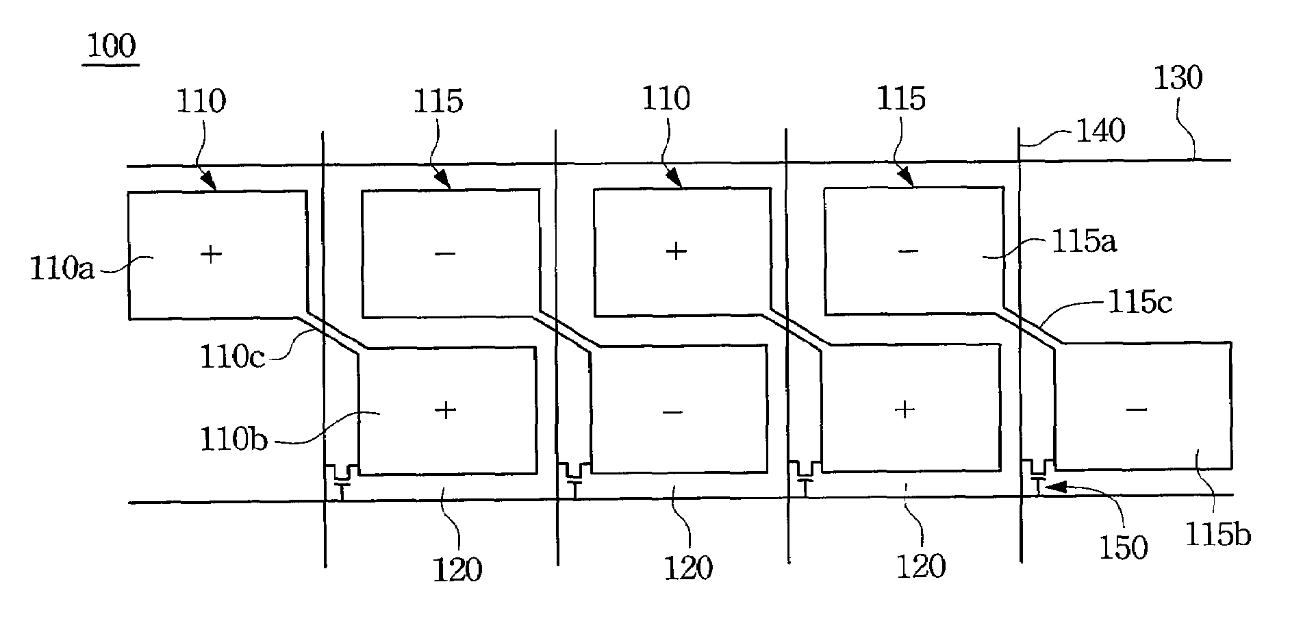
[0020]FIG. 1 illustrates the pixel array of an LCD according to an embodiment of the invention. The pixel array 100 comprises pixel electrodes 110 and 115. The pixel electrode 110 comprises two sub-pixel electrodes 110a and 110b. The sub-pixel electrodes 110a, 110b are formed in two neighboring pixel areas 120 sharing an edge and diagonally connected to each other through a connecting part 110c. Similarly, pixel electrode 115 comprises two sub-pixel electrodes 115a and 115b. The sub-pixel electrodes 115a and 115b are formed in two neighboring pixel areas 120 sharing an edge and diagonally connected to each other through a connecting part 115c. Therefore, a repeating unit of the pattern formed by the first sub-pixel electrodes 110a, 110b and the second sub-pixel electrodes 115a, 115b is two first sub-pixel electrodes 110a, 110b in the two diagonal areas of a parallelogram and two second sub-pixel electrodes 115a, 115b in the other two diagonal areas of the parallelogram.
[0021]Each of the above mentioned pixel area 120 is defined by a pair of scan lines 130 and a pair of data lines 140. A switch device 150 is formed in one corner of the pixel area 120. The switch device 150 of this embodiment is a thin film transistor with a gate, a source and a drain connected to the scan line 130, the data line 140, the sub-pixel electrode 110b or 115b, respectively.
[0022]The pixel electrodes 110, 115 shown in FIG. 1 are formed on a switch device substrate alternatively. The two neighboring pixel electrodes 110, 115 can be controlled to have opposite polarities, so that one pixel area 120 comprising two sub-pixel electrodes 110b, 115a (or 110a, 115b) with opposite polarities can be obtained. The sub-pixel electrodes 110b, 115a (or 110a, 115b) in one pixel area 120 belong to two different pixel electrodes 115, 110. Because, for example, the two sub-pixel electrodes (110a, 110b) or (115a, 115b) of one pixel electrode 110 or 115 are still connected to each other, only one switch device is required to drive the pixel electrodes 110, 115. In addition, dot inversion method or any appropriate method can be used to allow the two neighboring pixel electrodes 110, 115 to have opposite polarities.

Example

Embodiment 2
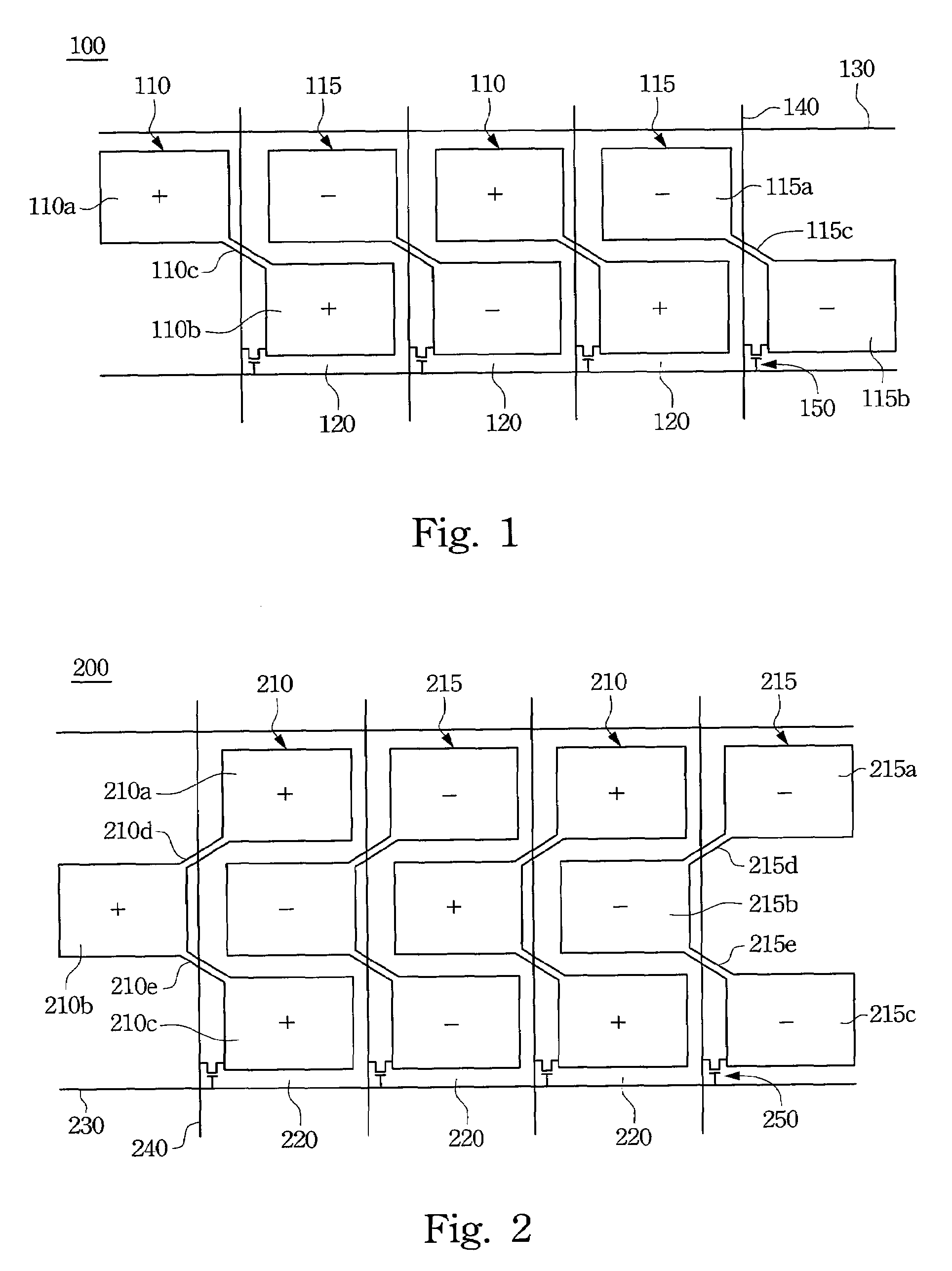
[0023]FIG. 2 illustrates the pixel array of an LCD according to another embodiment of the invention. FIG. 2 shows that pixel array 200 is composed of pixel electrodes 210 and 215. The pixel electrode 210 is divided into three sub-pixel electrodes 210a, 210b, and 210c. The sub-pixel electrodes 210a, 210b, and 210c are formed in the two neighboring pixel areas 220 sharing an edge. The sub-pixel electrode 210b is diagonally connected to the sub-pixel electrodes 210a and 210c through connecting parts 210d and 210e. Similarly, the pixel electrode 215 is divided into three sub-pixel electrodes 215a, 215b, and 215c. The sub-pixel electrodes 215a, 215b, and 215c are formed in the two neighboring pixel areas 22 sharing an edge. The sub-pixel electrode 215b is diagonally connected to sub-pixel electrodes 215a and 215c through connecting parts 215d and 215e. Therefore, a repeating unit of the pattern formed by, for example, the first sub-pixel electrodes 210a, 110b and the second sub-pixel electrodes 215a, 215b is two first sub-pixel electrodes 210a, 210b in the two diagonal areas of a parallelogram and two second sub-pixel electrodes 215a, 215b in the other two diagonal areas of the parallelogram.
[0024]Each of the above mentioned pixel area 220 is defined by a pair of scan lines 230 and a pair of data lines 240. In addition, a switch device 250 is formed in one corner of each pixel area 220. The switch device 250 in this embodiment is a thin film transistor with a gate, a source and a drain connected to the scan line 230, the data line 240 and the sub-pixel electrode 210c or 215c, respectively.
[0025]As shown in FIG. 2, the pixel electrodes 210 and 215 are alternatively formed on a switch device substrate. The three sub-pixel electrodes 210a, 215b, 210c (or 215a, 210b, 215c) within the same pixel area 220 have opposite polarities between the sub-pixel electrodes 210a, 210c (or 215a, 215c) and the sub-pixel electrode 215b (or 210b) when the neighboring pixel electrode 210 and the pixel electrode 215 have opposite polarities. Although the sub-pixel electrodes 210a, 210b 210c of the pixel electrode 210 are arranged in two pixel areas 220 sharing an edge, the sub-pixel electrodes 210a, 210b, 210c of the pixel electrode 210 are connected through the connecting parts 210d and 210e. Hence, only one switch device 250 is required for the pixel electrode 210. Similarly, the sub-pixel electrodes 215a, 215b, 215c of the pixel electrode 215 are also connected through the connecting parts 215d and 215e; hence only one switch device 250 is required for the pixel electrode 215. The way to obtain two neighboring pixel electrodes 210, 215 with opposite polarities can be, for example, dot inversion.

Example

Embodiment 3
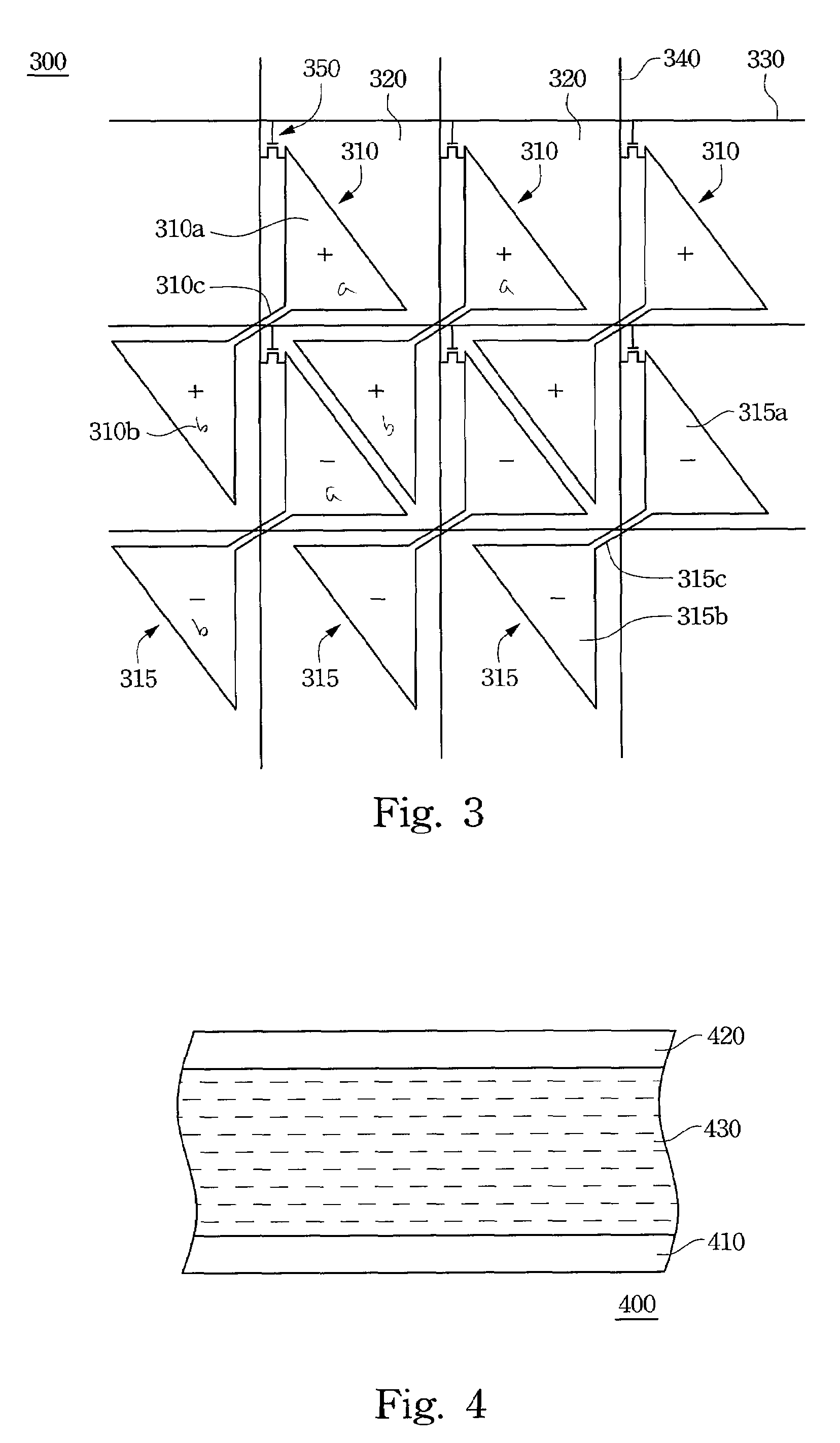
[0026]FIG. 3 illustrates the pixel array of an LCD according to another embodiment of the invention. The pixel array 300 is composed of pixel electrodes 310 and 315. The pixel electrode 310 is divided into two sub-pixel electrodes 310a and 310b located in two pixel areas 320 sharing a corner. The sub-pixel electrodes 310a and 310b are connected to each other through a connecting part 310c. Similarly, pixel electrode 315 comprises two sub-pixel electrodes 315a, 315b located in two pixel areas 320 sharing a corner. The sub-pixel electrodes 315a and 315b are connected to each other through a connecting part 315c. Therefore, a repeating unit of a pattern formed by the first sub-pixel electrodes 310a, 310b and the second sub-pixel electrodes 315a, 315b is two first sub-pixel electrodes 310a, 310b located in the two opposite edges of a parallelogram and two second sub-pixel electrodes 315a, 315b located in the other two opposite edges of the parallelogram.
[0027]The above mentioned pixel area 320 is defined by a pair of scan line 330 and a pair of data line 340. A switch device 350 is formed in one corner of the pixel area 320. The switch device 350 in this embodiment is a thin film transistor with a gate, a source and a drain connected to the scan line 330, the data line 340, the sub-pixel electrode 310a or 315a, respectively.
[0028]The pixel electrodes 310, 315 shown in FIG. 3 are formed on a switch device substrate alternatively. The two neighboring pixel electrodes 310, 315 can be controlled to have opposite polarities, so that the same pixel area 320 comprising two sub-pixel electrodes 310b, 315a (or 315b, 310a) with opposite polarities can be obtained. Although the two sub-pixel electrodes 310b, 315a (or 315b, 310a) in one pixel area 320 belong to two different pixel electrodes 315 and 310, the two sub-pixel electrodes 310a, 310b (or 315a, 315b) belonged the pixel electrode 310 (or 315) are still connected to each other through the connecting part 310c. Hence, only one switch device is required to drive the pixel electrode 310 (or 315). In addition, dot inversion method or any appropriate method can be used to allow the two neighboring pixel electrodes 310, 315 to have opposite polarities.
[0029]The above mentioned pixel array structure can be applied to any flat panel display, for example, LCD. Referring to FIG. 4, an LCD 400 comprises a lower substrate 410, an upper substrate 420 and a liquid crystal layer 430 disposed therebetween. There are many possible modifications for the lower substrate 410 and the upper substrate 420 of recent LCD 400 products. For the first example, the upper substrate 420 can be a color filter if the lower substrate 410 is a control circuit board. For the second example, the control circuit board and the color filter layer can be formed on the lower substrate 410, and there is only a common electrode layer on the upper substrate 420. Based on the location of the control circuit and the color filter, the structure can be either COA (Color Filter on Array) or AOC (Array on Color Filter). The detailed structures of COA and AOC are not shown in FIG. 4 because these possible modifications are apparent to those skilled in the art.
[0030]Accordingly, the pixel electrode is only divided into several structurally connected sub-pixel electrodes. Only one driving switch device is required for one pixel. Furthermore, pixel electrodes with opposite polarities are alternatively arranged. At least two sub-pixel electrodes can be formed on each pixel area without additional signal line and driving switch device.
[0031]It will be apparent to those skilled in the art that various modifications and variations can be made to the structures of the present invention without departing from the scope or spirit thereof. In view of the foregoing, it is intended that the present invention cover modifications and variations thereof provided they fall within the scope of the following claims.

PUM

no PUM

Description & Claims & Application Information

We can also present the details of the Description, Claims and Application information to help users get a comprehensive understanding of the technical details of the patent, such as background art, summary of invention, brief description of drawings, description of embodiments, and other original content. On the other hand, users can also determine the specific scope of protection of the technology through the list of claims; as well as understand the changes in the life cycle of the technology with the presentation of the patent timeline. Login to view more.
Why Eureka
Try Eureka