Charge pump circuit, LCD driver IC, and liquid crystal display device

Inactive Publication Date: 2007-09-20
ROHM CO LTD
View PDF5 Cites 6 Cited by
  • Summary
  • Abstract
  • Description
  • Claims
  • Application Information

AI Technical Summary

Benefits of technology

[0013] An object of the present invention is to provide charge pump circuits that can change their step-up factor finely and in a wide range without requiring an unnecessarily large number of step-up stages, and to provide LCD driver ICs and liquid crystal display devices incorporating such charge pump circuits.

Problems solved by technology

Thus, a disadvantage with the conventional charge pump circuits is that their step-up factor can be selected only among values that form an arithmetic progression with a common difference equal to the just mentioned step-up input voltage (e.g., among factors of 2, 4, 6, 8, and so forth).
This requirement, however, is not met by the conventional charge pump circuits described above.
Simply setting the step-up input voltage low, however, necessitates an accordingly large number of step-up units (and hence an accordingly large number of externally fitted charge-transfer capacitors with which they are built).
This leads to an unduly large circuit scale and an unduly high cost, making it impracticable to set the step-up input voltage low.

Method used


Image

  • Charge pump circuit, LCD driver IC, and liquid crystal display device
  • Charge pump circuit, LCD driver IC, and liquid crystal display device
  • Charge pump circuit, LCD driver IC, and liquid crystal display device

Examples


first embodiment

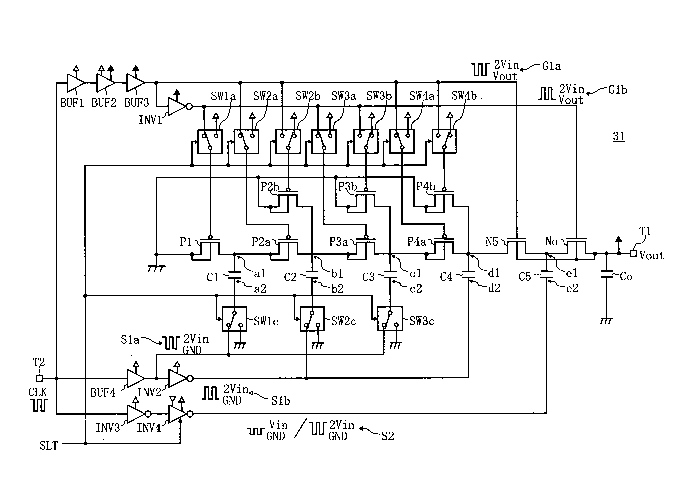
[0036] First, as the invention, an example of the negative step-up charge pump circuit included in the power supply circuit 31 will be described in detail below, with reference to FIG. 3.

[0037]FIG. 3 is a circuit block diagram of the power supply circuit 31 (and in particular the negative step-up charge pump circuit included in it) according to the first embodiment.

[0038] As shown in FIG. 3, in this embodiment, the negative step-up charge pump circuit includes charge transfer transistors P1, P2a, P2b, P3a, P3b, P4a, P4b, and N5, an output transistor No, charge transfer capacitor C1 to C5, an output capacitor Co, buffers BUF1 to BUF4, inverters INV1 to INV4, and switches SW1a, SW1c, SW2a, SW2b, SW2c, SW3a, SW3b, SW3c, SW4a, and SW4b. In addition to this negative step-up charge pump circuit, the power supply circuit 31 of this embodiment further includes a positive step-up charge pump circuit (unillustrated) that produces from the input voltage Vin a positively stepped-up voltage 2Vi...

second embodiment

[0082] Next, as the invention, another example of the negative step-up charge pump circuit included in the power supply circuit 31 will be described in detail below, with reference to FIG. 5.

[0083]FIG. 5 is a circuit block diagram of the power supply circuit 31 (and in particular the negative step-up charge pump circuit included in it) according to the second embodiment.

[0084] The negative step-up charge pump circuit of this embodiment, like that of the first embodiment described above, is configured as a charge pump circuit that negatively steps up an input voltage Vin to produce a desired output voltage Vout with a plurality of stages of step-up units built with charge transfer transistors and charge transfer capacitors, and includes a first controller (of which no part is illustrated here that is the same as in the first embodiment) for increasing and decreasing the number of stages of step-up units actually operated according to the step-up factor specified. The difference here...


PUM


Abstract

A charge pump circuit has a first controller (in the embodiments, switches SW1a to SW4b and charge transfer transistors P2b to P4b) that increases and decreases the number of step-up units actually operated according to the specified step-up factor; and a second controller (in the embodiments, an inverter INV4) varies the step-up input voltage in one of the step-up units according to the specified step-up factor. With this configuration, it is possible to vary the step-up factor finely and in a wide range without unnecessarily increasing the number of step-up stages.

Description

[0001] This application is based on Japanese Patent Application No. 2006-077148 filed on Mar. 20, 2006, the contents of which are hereby incorporated by reference. BACKGROUND OF THE INVENTION [0002] 1. Field of the Invention [0003] The present invention relates to charge pump circuits that step up an input voltage to produce a desired output voltage, and to LCD driver ICs and liquid crystal display devices incorporating such charge pump circuits. [0004] 2. Description of Related Art [0005] Conventionally, charge pump circuits are known that produce a desired output voltage by positively or negatively stepping up an input voltage through a plurality of stages of step-up units built with charge transfer transistors and charge transfer capacitors. [0006] Some conventionally known charge pump circuits are capable of changing their step-up factor by increasing or decreasing the number of stages of step-up units actually operated. [0007] As an example of a conventional technology related ...

Claims


Application Information

Patent Timeline
IPC IPC(8): G09G3/36
CPCG09G3/3648G09G2330/02G09G2320/041G09G3/3696
Inventor NAGAI, TAKASHIITO, AKITO
Owner ROHM CO LTD
Why Eureka
Try Eureka