Front-end signal processing circuit and imaging device

a signal processing circuit and imaging device technology, applied in the field of front-end signal processing circuit and imaging device, can solve the problems of error generation, image becomes darker than an original image, and output corresponding to original signal level of effective pixel region cannot be obtained

Inactive Publication Date: 2007-09-20
COLLABO INNOVATIONS INC
View PDF15 Cites 11 Cited by
  • Summary
  • Abstract
  • Description
  • Claims
  • Application Information

AI Technical Summary

Benefits of technology

[0015] The front-end signal processing circuit and the imaging device including the front-end signal processing circuit of the present invention, correct the difference between the black level of the digital luminance signal corresponding to the effective pixel region after clamping and the prescribed set level based on the digital luminance signal corresponding to the OB region. Therefore, the black level of the output signal of the image sensor can be stabilized in the prescribed set level, without being influenced by the DC offset component of the circuit elements making up the feedback loop.

Problems solved by technology

However, since the DC offset component is usually included in these circuit elements, an error is generated by an influence of the DC offset component, and the black level of the output signal corresponding to the effective pixel region is not equal to the set level.
Therefore, there is a problem that an output corresponding to an original signal level of the effective pixel region can not be obtained.
For example, when a difference between the signal level of the effective pixel region and the black level becomes small by the DC offset component, there is a problem that an image becomes darker than an original image.
Therefore, there is a problem that an output obtained in the DSP becomes far removed from the original signal level of the effective pixel region.

Method used


Image

  • Front-end signal processing circuit and imaging device
  • Front-end signal processing circuit and imaging device
  • Front-end signal processing circuit and imaging device

Examples


Embodiment Construction

[0021] Preferred embodiments of the present invention will be explained, with reference to the drawings hereunder.

[1.1] Configuration of an Imaging Device

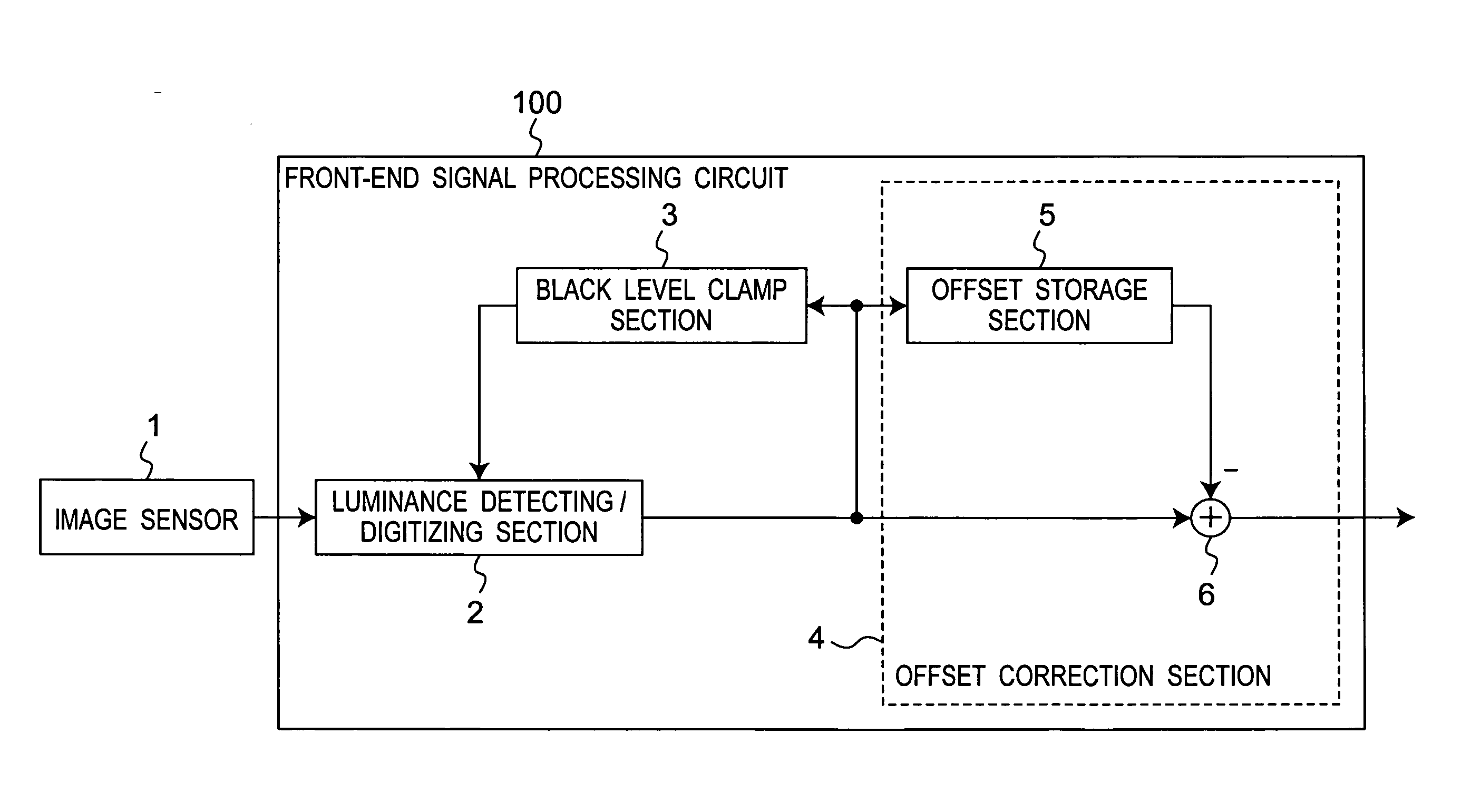
[0022]FIG. 1 shows a configuration of an imaging device of an embodiment of the present invention. The imaging device of the embodiment has an image sensor 1 and a front-end signal processing circuit 100 that processes an output signal of the image sensor 1. The front-end signal processing circuit 100 is made up of a semiconductor integrated circuit (IC).

[0023] The front-end signal processing circuit 100 has a luminance detecting / digitizing section 2 that detects luminance information included in the output signal of the image sensor 1 to clamp a black level of the luminance information to a prescribed set level based on a feedback voltage being a clamp level and converts the luminance information into a digital luminance signal; and a black level clamp section 3 that makes up a feedback loop together with the luminance detectin...


PUM


Abstract

A front-end signal processing circuit that stabilizes a black level of an output signal of an image sensor in a prescribed set level, without being influenced by a DC offset component of circuit elements making up a feedback loop, and an imaging device including such the front-end signal processing circuit, are provided. The front-end signal processing circuit includes a feedback loop made up of a luminance detecting/digitizing section and a black level clamp section, and clamps a black level of an output signal of an image sensor to a prescribed set level. The front-end signal processing circuit further includes an offset correction section. The offset correction section stores an offset value being a difference between a signal level of an OB region of the image sensor and the prescribed level, subtracts the offset value from a digital luminance signal corresponding to an effective pixel region of the image sensor, and outputs the obtained signal.

Description

BACKGROUND OF THE INVENTION [0001] 1. Field of the Invention [0002] The present invention relates to a front-end signal processing circuit that processes an analog signal outputted from an image sensor, and an imaging device including such the front-end signal processing circuit. [0003] 2. Related Art [0004] The analog signal outputted from an image sensor such as a CCD (Charge Coupled Device) is first processed by the front-end signal processing circuit, and is outputted to a DSP (Digital Signal Processor) at the following stage. JP-A-2001-189892 discloses an imaging device having the image sensor and the front-end signal processing circuit. The image sensor has an effective pixel region in which light from an object is received and photoelectric conversion of the light is performed, and an optical black region (hereinafter referred to as an “OB region”) being an optical black area in which the photoelectric conversion is not performed, and the imaging device outputs an output sign...

Claims


Application Information

Patent Timeline
Patent Type & Authority Applications(United States)
IPC IPC(8): H04N5/228
CPCH04N5/3575H04N5/3655H04N5/361H04N25/616H04N25/673H04N25/63
Inventor HATANI, NAOHISAOTANI, MITSUHIKOYAMAGUCHI, KOUJI
Owner COLLABO INNOVATIONS INC
Why Eureka
Try Eureka