

Thermally printable electrically conductive ribbon and method
a technology thermal printing, which is applied in the field of thermal printing of electrically conductive ribbons, can solve the problems of volatile chemicals presently known and used for fabricating screens, time-consuming and labor-intensive silkscreen processes, and inability to meet the requirements of use, so as to avoid the time and expense of silkscreen processes
- Summary
- Abstract
- Description
- Claims
- Application Information
AI Technical Summary
Benefits of technology
Problems solved by technology
Method used
Image

Examples
Embodiment Construction
[0019] While the present invention is susceptible of embodiment in various forms, there is shown in the figures and will hereinafter be described a presently preferred embodiment with the understanding that the present disclosure is to be considered an exemplification of the invention and is not intended to limit the invention to the specific embodiment illustrated.
[0020] It should be further understood that the title of this section of this specification, namely, “Detailed Description Of The Invention”, relates to a requirement of the United States Patent Office, and does not imply, nor should be inferred to limit the subject matter disclosed herein.
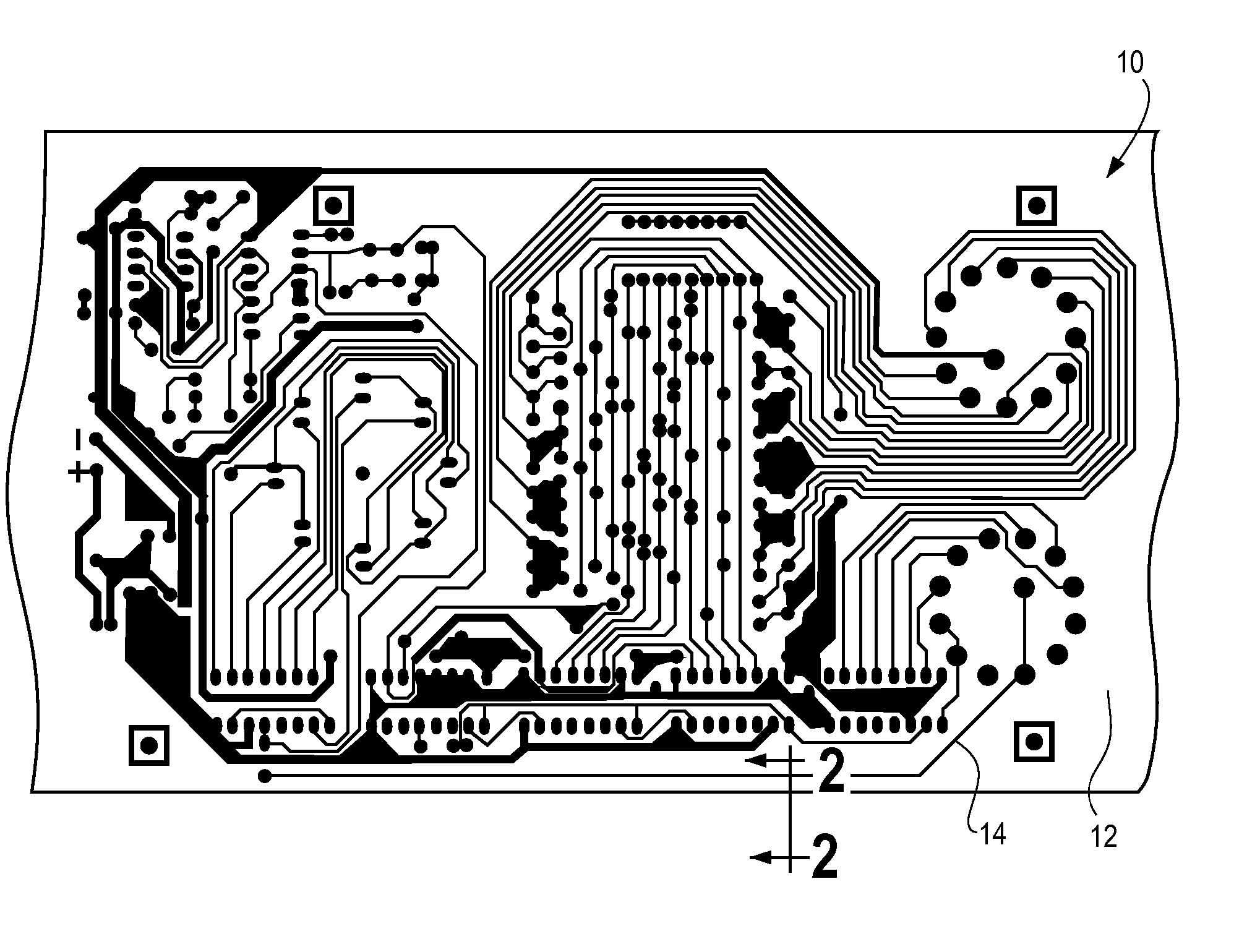
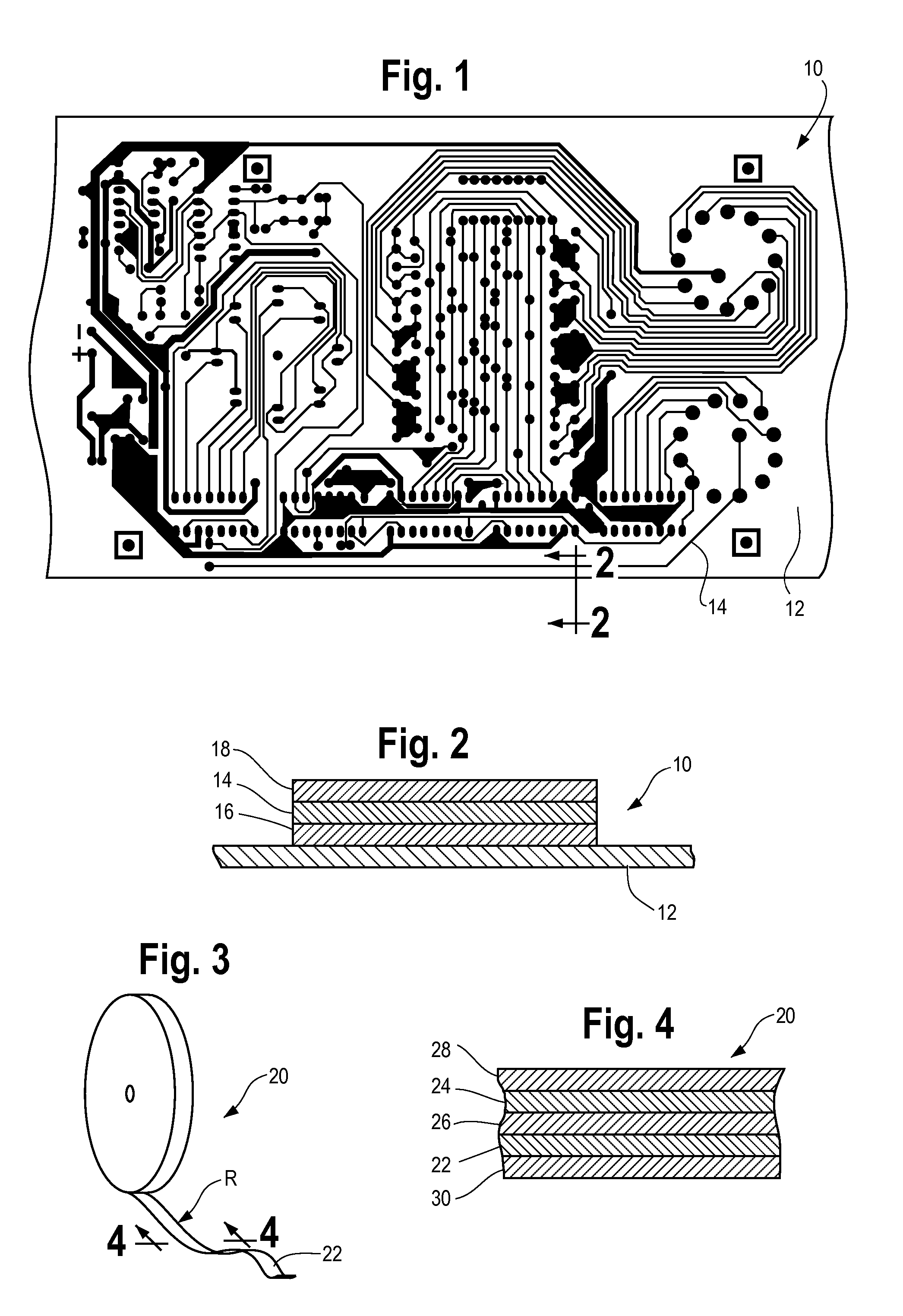
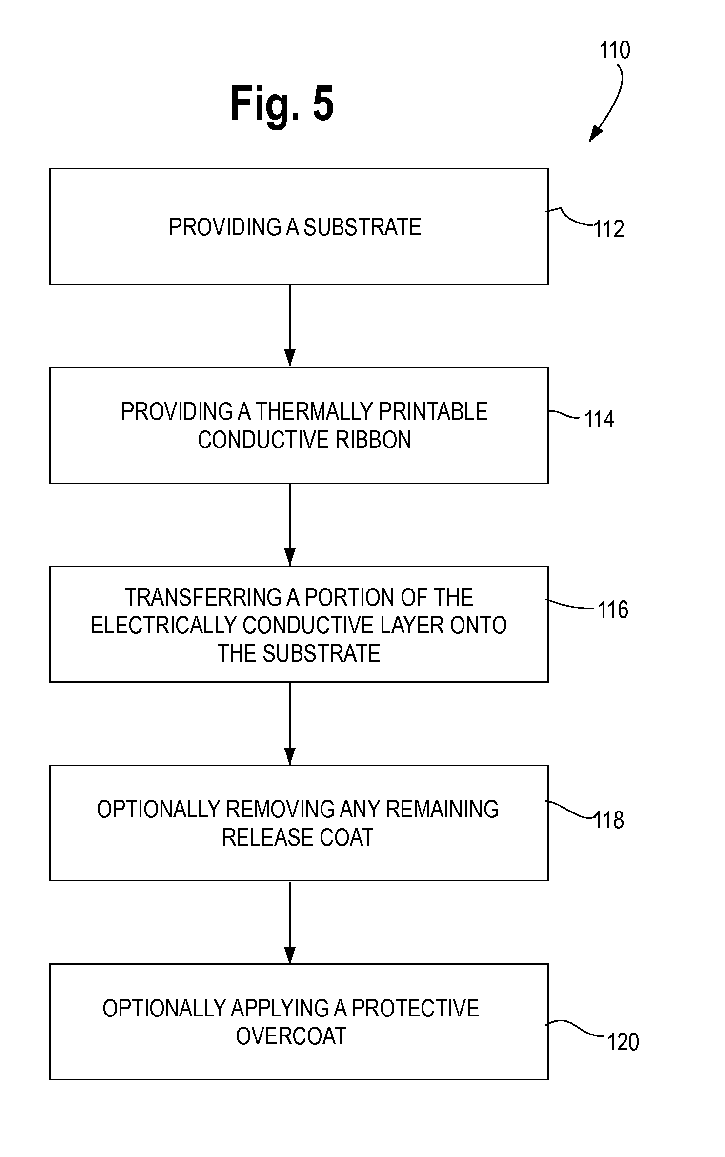
[0021] The present invention permits the fabrication of flexible circuitry using thermal transfer processes. Advantageously, the present invention eliminates the need for expensive silkscreen processes, and their attendant drawbacks.
[0022] Referring to the FIG. 1, there is shown an exemplary flexible circuit 10 formed in accordance w...
PUM
 Abstract
Description
Claims
Application Information