Package structure

a technology of packaging and sealing shell, applied in the direction of semiconductor devices, semiconductor/solid-state device details, electrical devices, etc., can solve the problems of inability to precisely control the amount of sealing shell applied to the inner or outer sides of the spacer wall, inability to reduce and poor adhesion and airtight performance. achieve the effect of reducing the usage of sealing shell

Active Publication Date: 2007-09-27
ADVANCED SEMICON ENG INC
View PDF5 Cites 48 Cited by
  • Summary
  • Abstract
  • Description
  • Claims
  • Application Information

AI Technical Summary

Benefits of technology

[0011] It is an object of the present invention to provide a package structure that ca...

Problems solved by technology

Although the method and structure disclosed in the Taiwan Patent Number 1222705 can effectively control the gap between two substrates and prevent the active region from contamination, the sealant is flowable and thus the...

Method used


Image

  • Package structure
  • Package structure
  • Package structure

Examples


Embodiment Construction

[0021] While the present invention is susceptible of embodiment in various forms, there is shown in the drawings and will hereinafter be described a presently preferred embodiment with the understanding that the present disclosure is to be considered an exemplification of the invention and is not intended to limit the invention to the specific embodiment illustrated.

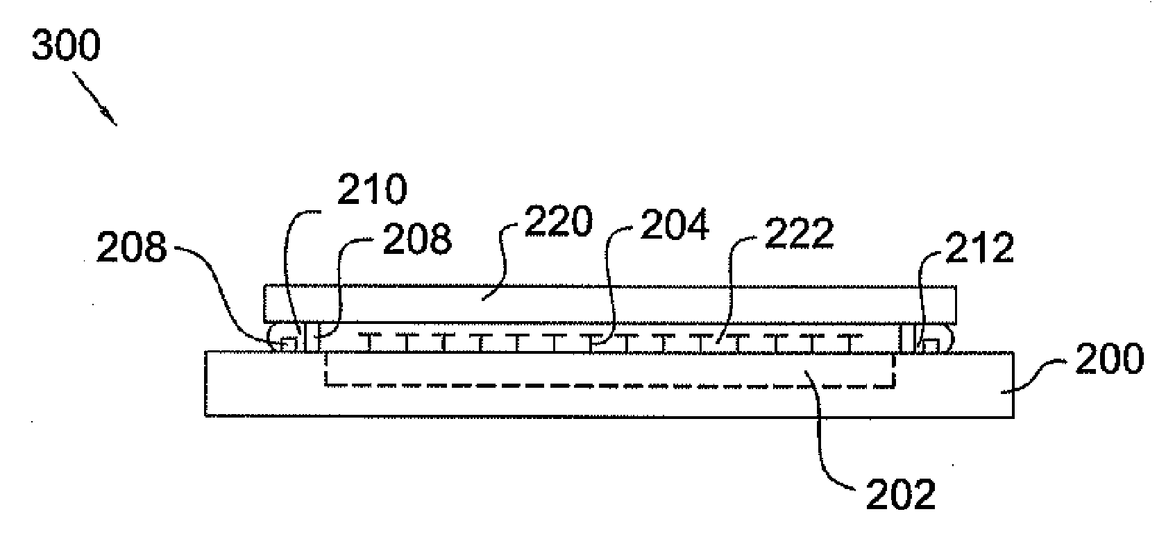
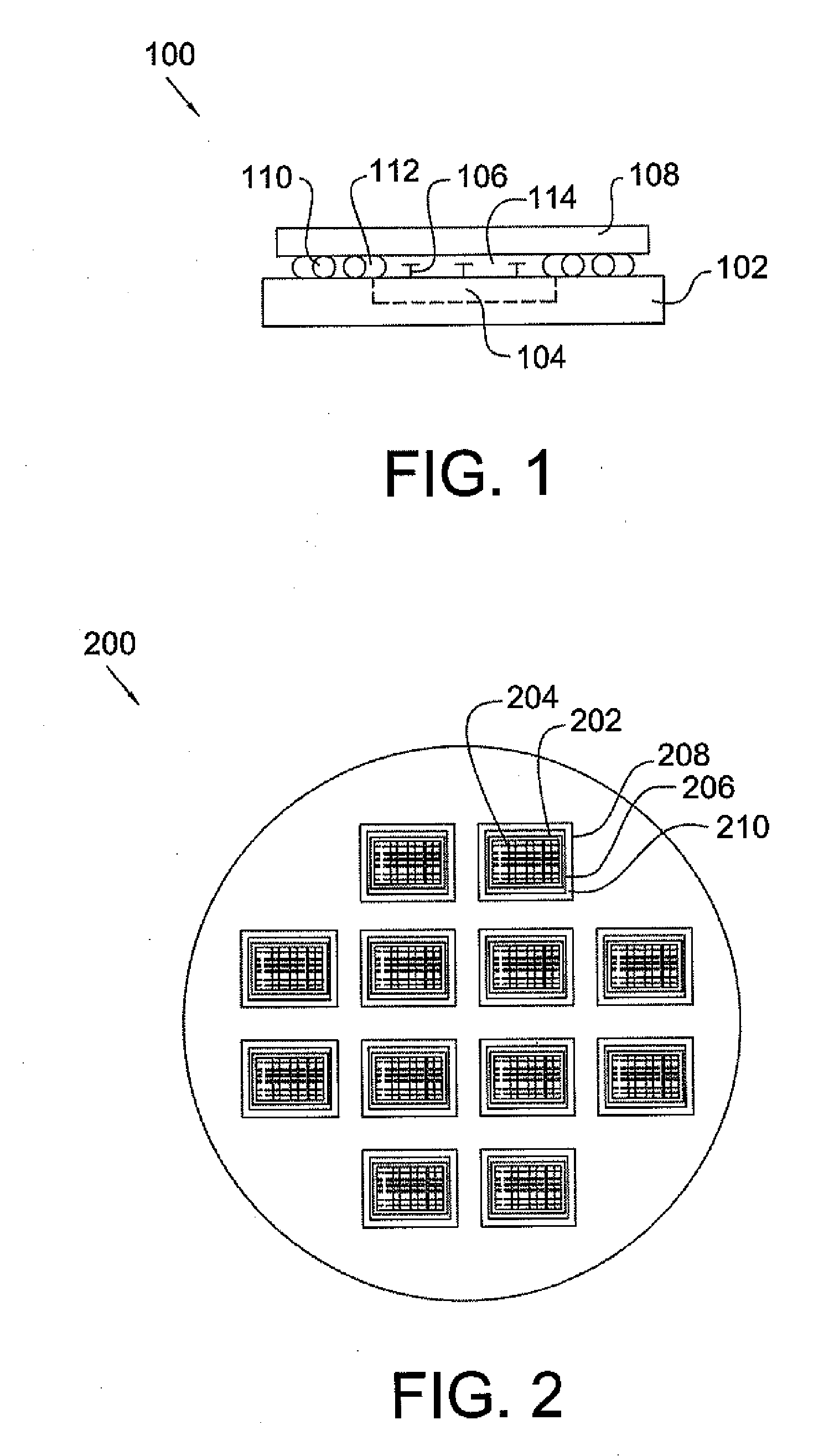
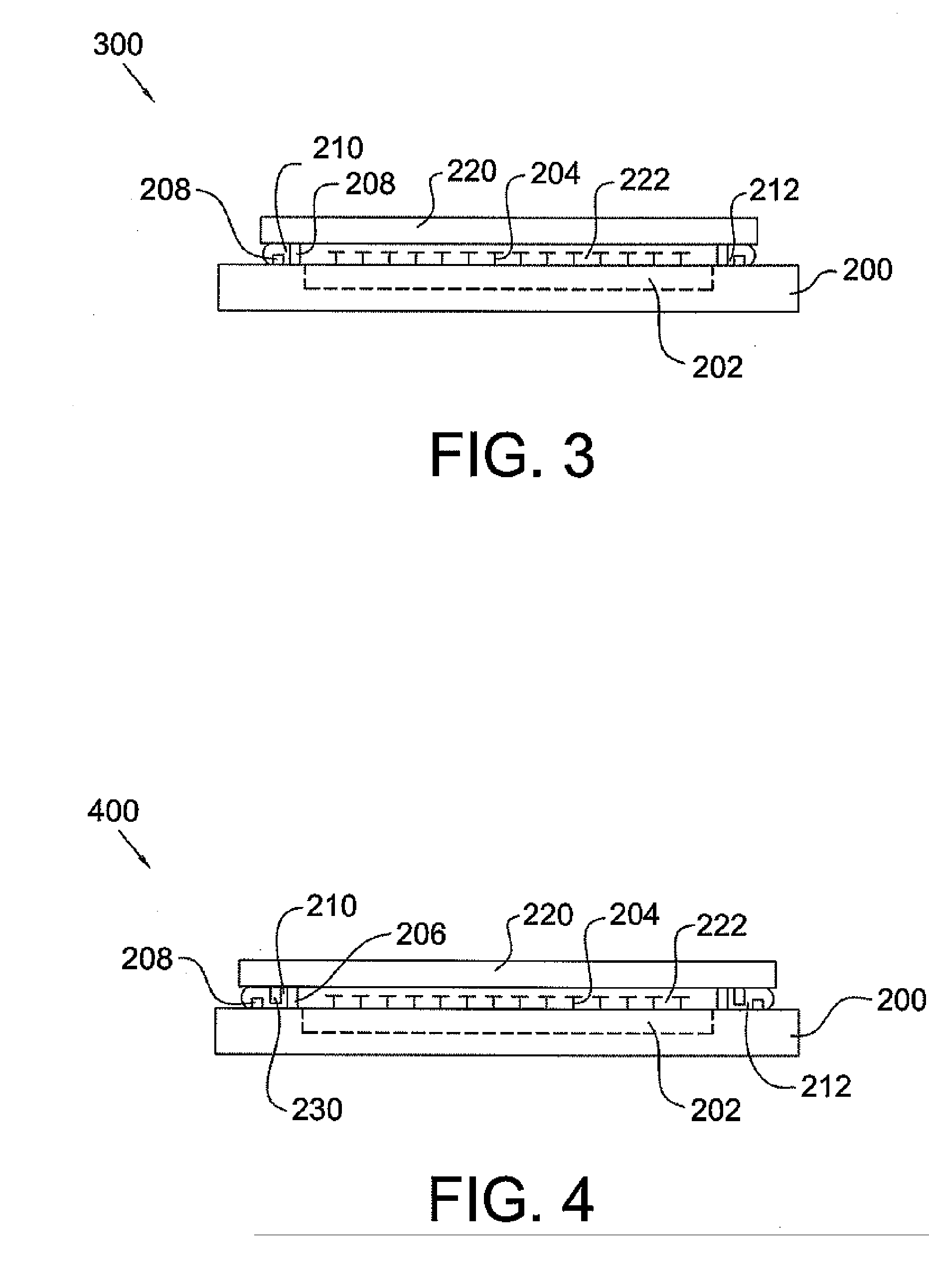
[0022] Referring to FIG. 2, it illustrates the top view of a substrate 200 according to an embodiment of the present invention. The substrate 200 such as a semiconductor wafer has an upper surface defining at least one predetermined area 202. At least one device 204 is disposed on the predetermined area 202. Therefore, the predetermined area 202 can be referred to as a device area. The device 204 can be a semiconductor device, MEMS device, optoelectronic device or other electronic devices.

[0023] In this embodiment, the device 204 is a CMOS device / MEMS device as an exemplary example to this embodiment. A first seal ring...


PUM


Abstract

A package structure is provided herein. The package structure includes a first substrate and a second substrate. A first seal ring having a first height is disposed around a predetermined area of the first substrate and between the first and second substrates. A second seal ring having a second height is disposed on the first substrate and around the first seal ring. A sealant is provided between the first and second seal rings to seal up the package structure.

Description

CROSS REFERENCE TO RELATED APPLICATION [0001] This application claims the priority benefit of Taiwan Patent Application Serial Number 095110365 filed Mar. 24, 2006, the full disclosure of which is incorporated herein by reference. BACKGROUND OF THE INVENTION [0002] 1. Field of the Invention [0003] The present invention relates to a package structure, and more particularly, to a package structure that has an enhanced adhesion and airtight performance, a reduced usage of applied sealant and can prevent the active region from contamination. [0004] 2. Description of the Related Art [0005] As the electronic devices, such as semiconductor devices, MicroElectroMechanical Systems (MEMS) devices and optoelectronic devices are becoming more and smaller, the circuitry therein used to drive these devices gets more compact accordingly. In order to isolate the devices from contamination such as dust, salt, grease or moisture to extend their lifespan and raise the reliability, the devices are requ...

Claims


Application Information

Patent Timeline
IPC IPC(8): H01L23/02
CPCB81B7/0041B81C2203/0118B81C2203/019H01L23/10H01L2924/1461H01L2224/16H01L2924/00
Inventor HUANG, CHENG WEI
Owner ADVANCED SEMICON ENG INC
Why Eureka
Try Eureka