Substrate treatment apparatus and substrate treatment method

a substrate treatment and treatment method technology, applied in the direction of carpet cleaners, instruments, photosensitive materials, etc., can solve the problem of insufficient cleaning at the portion

Inactive Publication Date: 2007-10-04
DAINIPPON SCREEN MTG CO LTD
View PDF12 Cites 16 Cited by
  • Summary
  • Abstract
  • Description
  • Claims
  • Application Information

AI Technical Summary

Benefits of technology

[0012]An object of the present invention is to provide a substrate treatment apparatus and a substrate treatment method capable of satisfactorily cleaning the peripheral end face of a substrate, regardless of the position of the substrate with respect to a brush.

Problems solved by technology

As a result, there is a fear of causing insufficient cleaning at the portion to which the brush is pushed relatively weakly.

Method used


Image

  • Substrate treatment apparatus and substrate treatment method
  • Substrate treatment apparatus and substrate treatment method
  • Substrate treatment apparatus and substrate treatment method

Examples


Embodiment Construction

[0037]Embodiments according to the present invention will be described below in detail referring to the accompanying drawings.

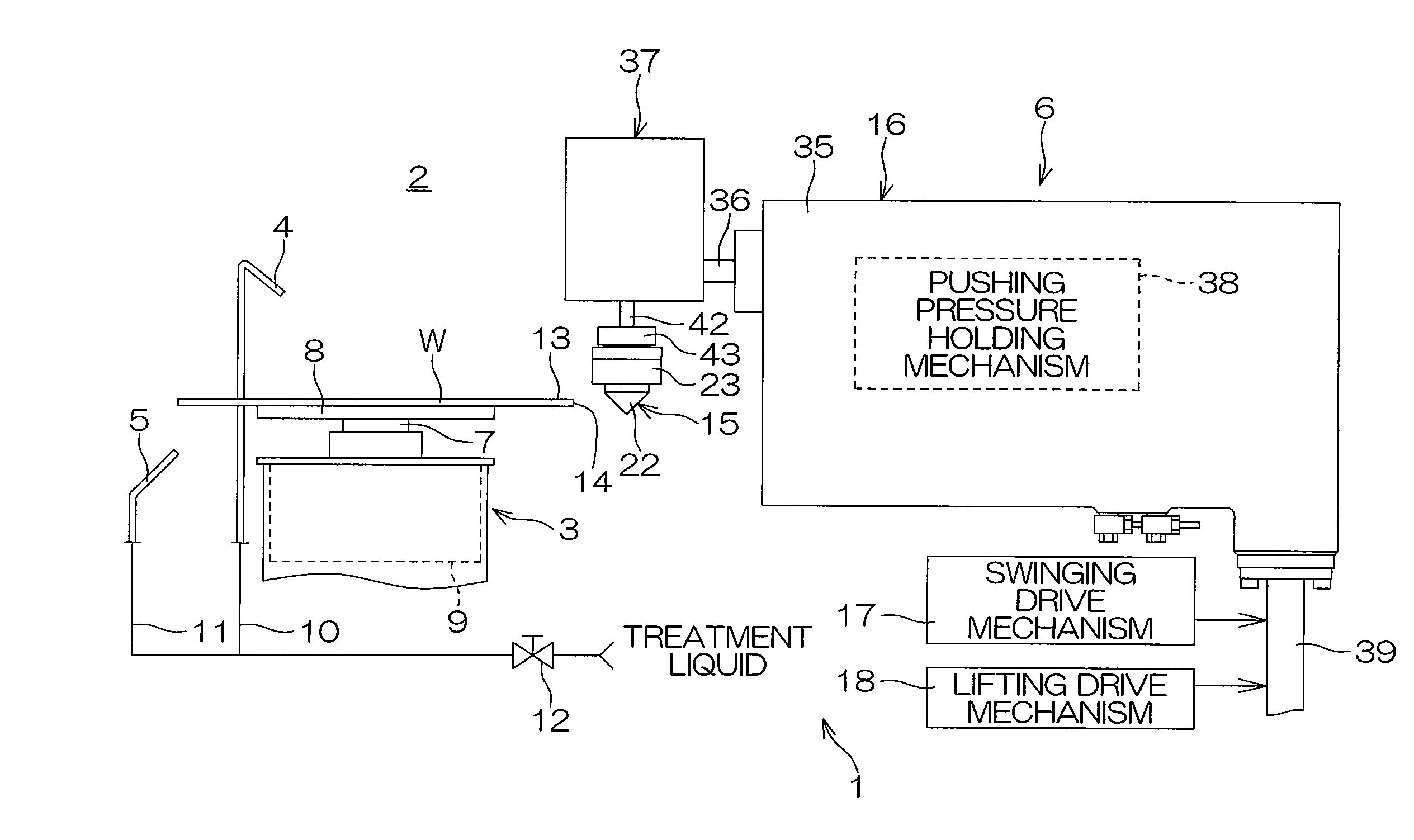
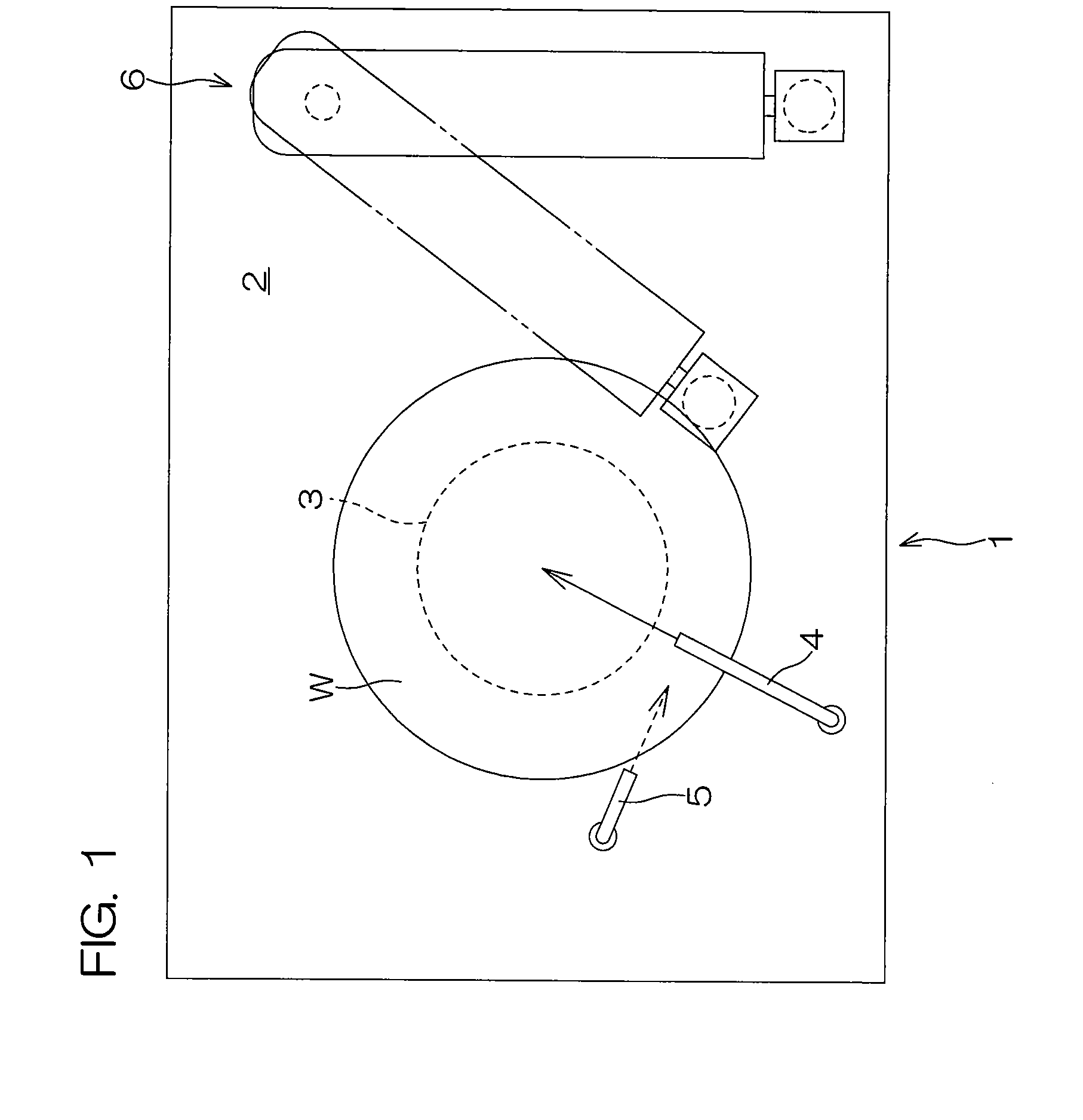
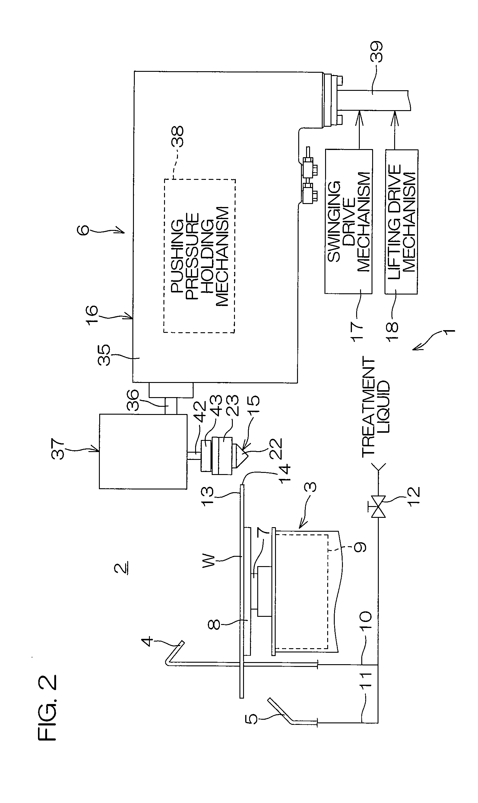
[0038]FIG. 1 is a plan view showing the schematic configuration of a substrate treatment apparatus according to an embodiment of the present invention. FIG. 2 is an illustrative side view showing the interior of the substrate treatment apparatus shown in FIG. 1.

[0039]This substrate treatment apparatus 1 is of a single wafer processing type for processing semiconductor wafers W (hereinafter referred to simply as “wafer W”) as an example of a substrate one by one. The substrate treatment apparatus 1 includes a spin chuck 3 for holding a wafer W generally horizontally and rotating it, a front surface nozzle 4 for supplying a treatment liquid to the front surface (the surface on which devices are formed) of the wafer W, a back surface nozzle 5 for supplying a treatment liquid to the back surface of the wafer W, and a brushing mechanism 6 for cleaning the peripher...


PUM


Abstract

A substrate treatment apparatus of the present invention includes a substrate holding mechanism for holding a substrate, a brush made of an elastically deformable material and having a cleaning surface intersecting a parallel direction along one surface of the substrate held by the substrate holding mechanism, a brush moving mechanism for moving the brush with respect to the substrate held by the substrate holding mechanism, a control unit for controlling the brush moving mechanism so that the cleaning surface is made to contact with the peripheral end face of the substrate held by the substrate holding mechanism, and a pushing pressure holding mechanism for holding the pushing pressure of the brush to the peripheral end face of the substrate in the parallel direction at a preset pushing pressure.

Description

BACKGROUND OF THE INVENTION[0001]1. Field of the Invention[0002]The present invention relates to a substrate treatment apparatus and a substrate treatment method for cleaning substrates. Substrates to be treated include semiconductor wafers, substrates for liquid crystal displays, substrates for plasma displays, substrates for FEDs (Field Emission Displays), substrates for optical discs, substrates for magnetic discs, substrates for magneto-optical discs, substrates for photomasks, etc.[0003]2. Description of Related Art[0004]In semiconductor device manufacturing processes, contaminants attached to the peripheral portion of a semiconductor wafer may have nonnegligible influence on the quality of the treated semiconductor wafer.[0005]In the so-called batch treatment process, multiple semiconductor wafers are held in a vertical posture and immersed in treatment liquid. Hence, if contaminants are attached to the peripheral portion of each semiconductor wafer, the contaminants are dispe...

Claims


Application Information

Patent Timeline
Patent Type & Authority Applications(United States)
IPC IPC(8): B08B1/04
CPCB08B1/04H01L21/67046H01L21/02087H01L21/304
Inventor HIRAOKA, NOBUYASUOKUMURA, TSUYOSHINAKANO, AKIYOSHI
Owner DAINIPPON SCREEN MTG CO LTD
Why Eureka
Try Eureka