

Printed circuit board using bump and method for manufacturing thereof
- Summary
- Abstract
- Description
- Claims
- Application Information
AI Technical Summary
Benefits of technology
Problems solved by technology
Method used
Image

Examples
Embodiment Construction
[0037]Embodiments of the printed circuit board using bumps and manufacturing method thereof, according to aspects of the invention, will be described below in more detail with reference to the accompanying drawings.
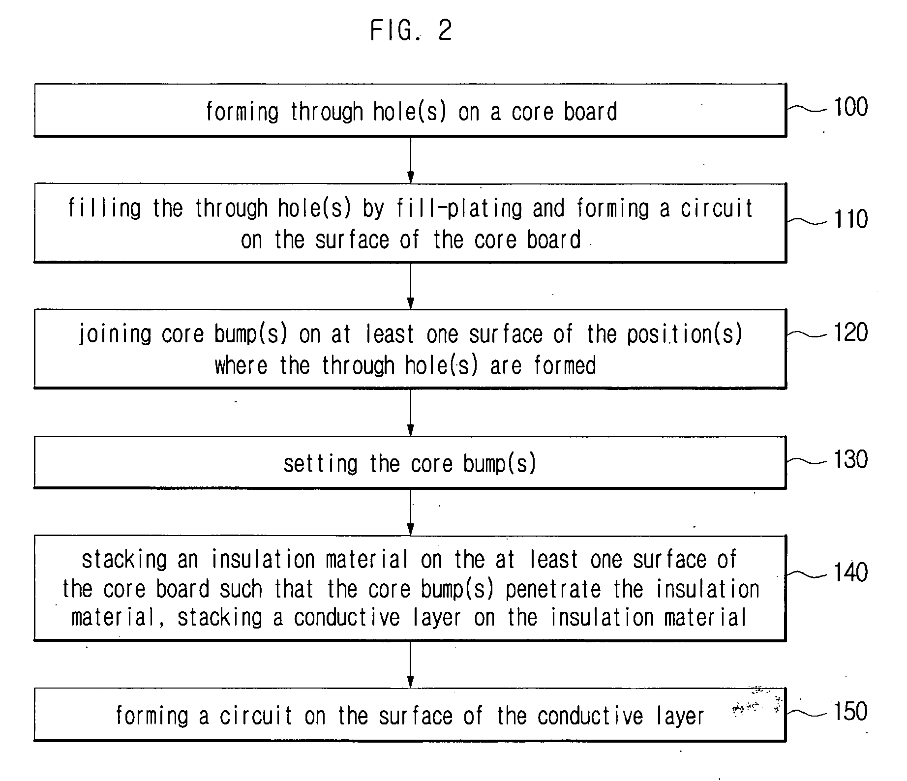
[0038]FIG. 2 is a flowchart illustrating a method of manufacturing a printed circuit board using bumps according to an embodiment of the present invention.
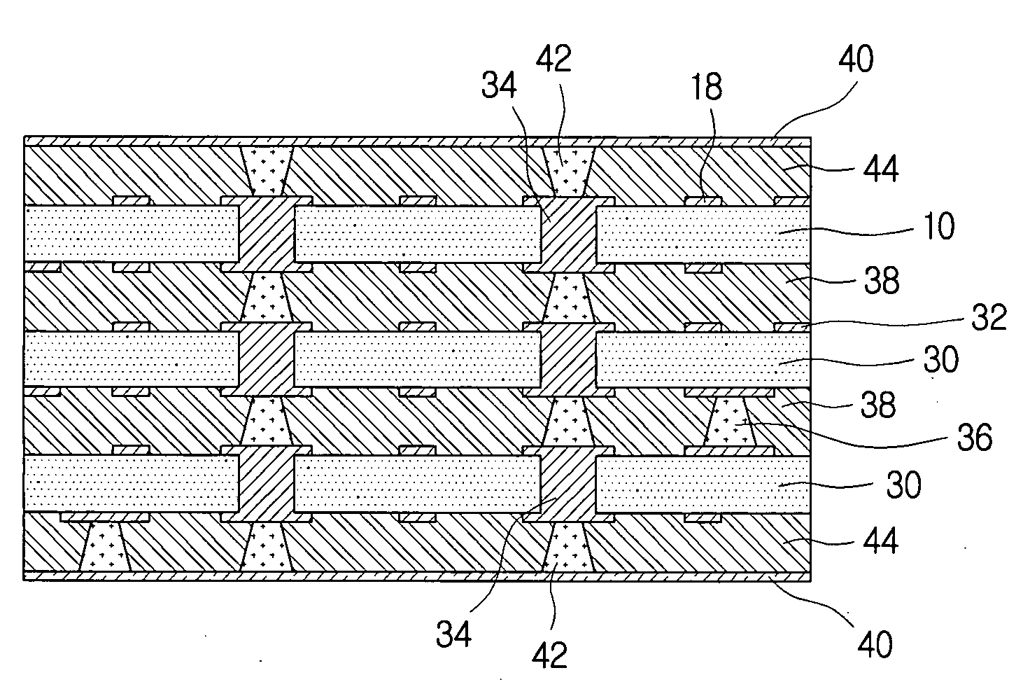
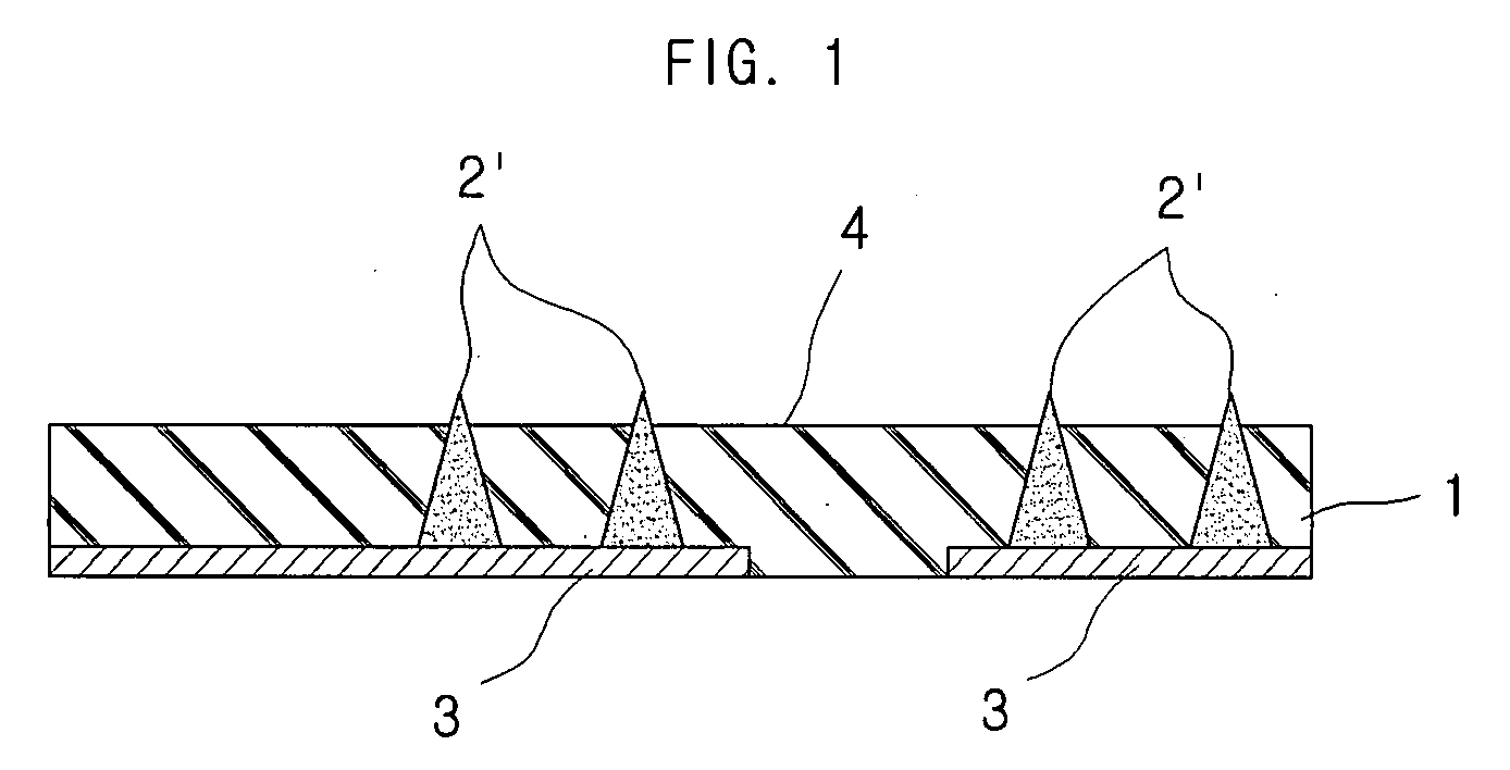
[0039]The present invention provides a core board which allows collectively manufacturing a multi-layer printed circuit board by forming through holes in the core board, filling the through holes by reverse pulse plating, printing core bumps in correspondence with the positions of the through holes, and stacking an insulation material. Accordingly, the printed circuit board may be formed, which allows forming a thick core board and forming bumps on the thick insulation layer, endures against pressure produced during the stacking process, is convenient for joining layers, exhibits excellent heat-releasing effect, allows ...
PUM
| Property | Measurement | Unit |
|---|---|---|
| Time | aaaaa | aaaaa |
| Time | aaaaa | aaaaa |
| Time | aaaaa | aaaaa |
Abstract
Description
Claims
Application Information