Wiring board in which silver is deposited near via-conductor and method for manufacturing wiring board

Inactive Publication Date: 2007-10-11
ALPS ALPINE CO LTD
View PDF7 Cites 5 Cited by
  • Summary
  • Abstract
  • Description
  • Claims
  • Application Information

AI Technical Summary

Benefits of technology

[0032]This allows the silver d

Problems solved by technology

Since the boehmite layer 54 and the polyimide layer 55 need to be partly removed by grinding such that the ceramic substrate 51 and the via-conductor

Method used


Image

  • Wiring board in which silver is deposited near via-conductor and method for manufacturing wiring board
  • Wiring board in which silver is deposited near via-conductor and method for manufacturing wiring board
  • Wiring board in which silver is deposited near via-conductor and method for manufacturing wiring board

Examples


Example

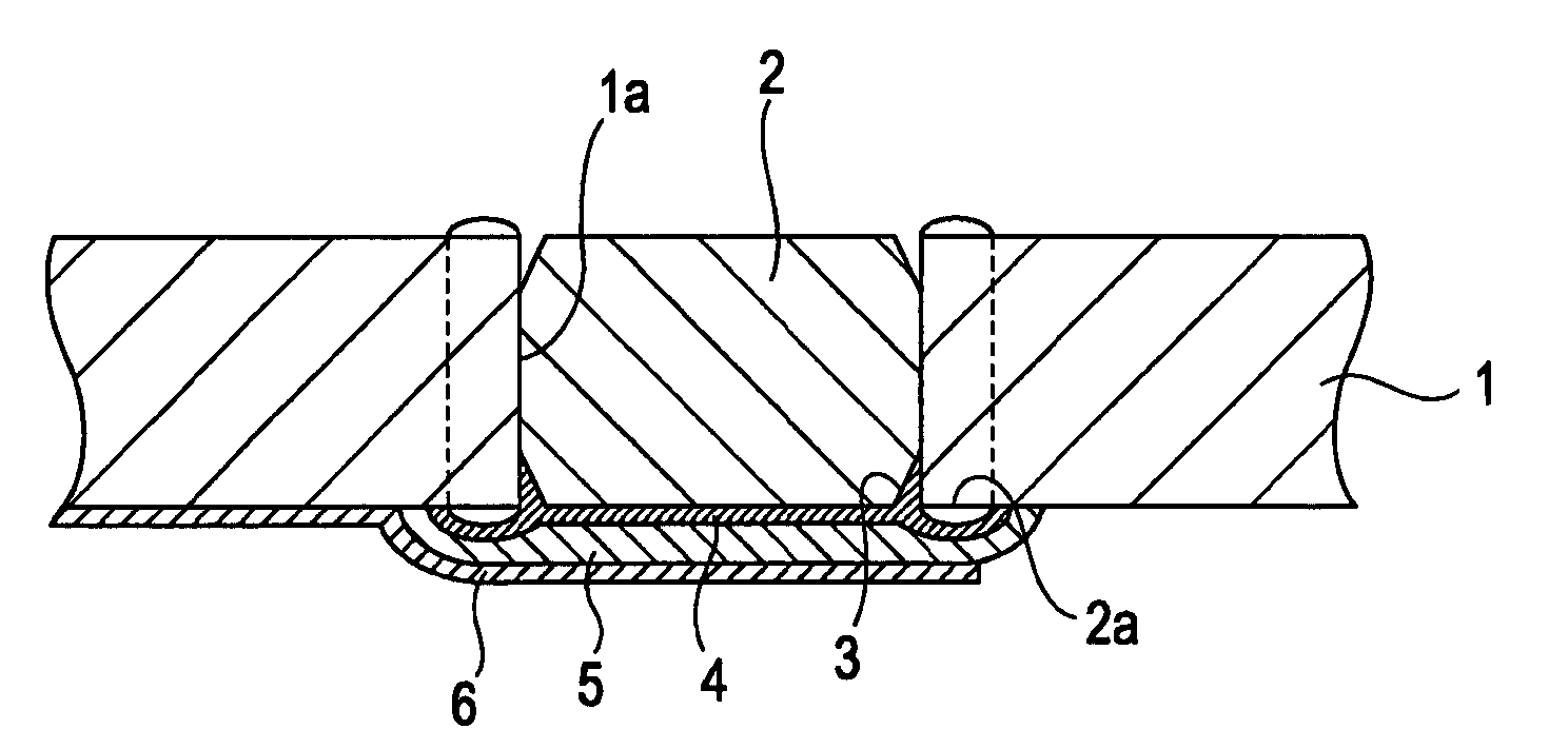
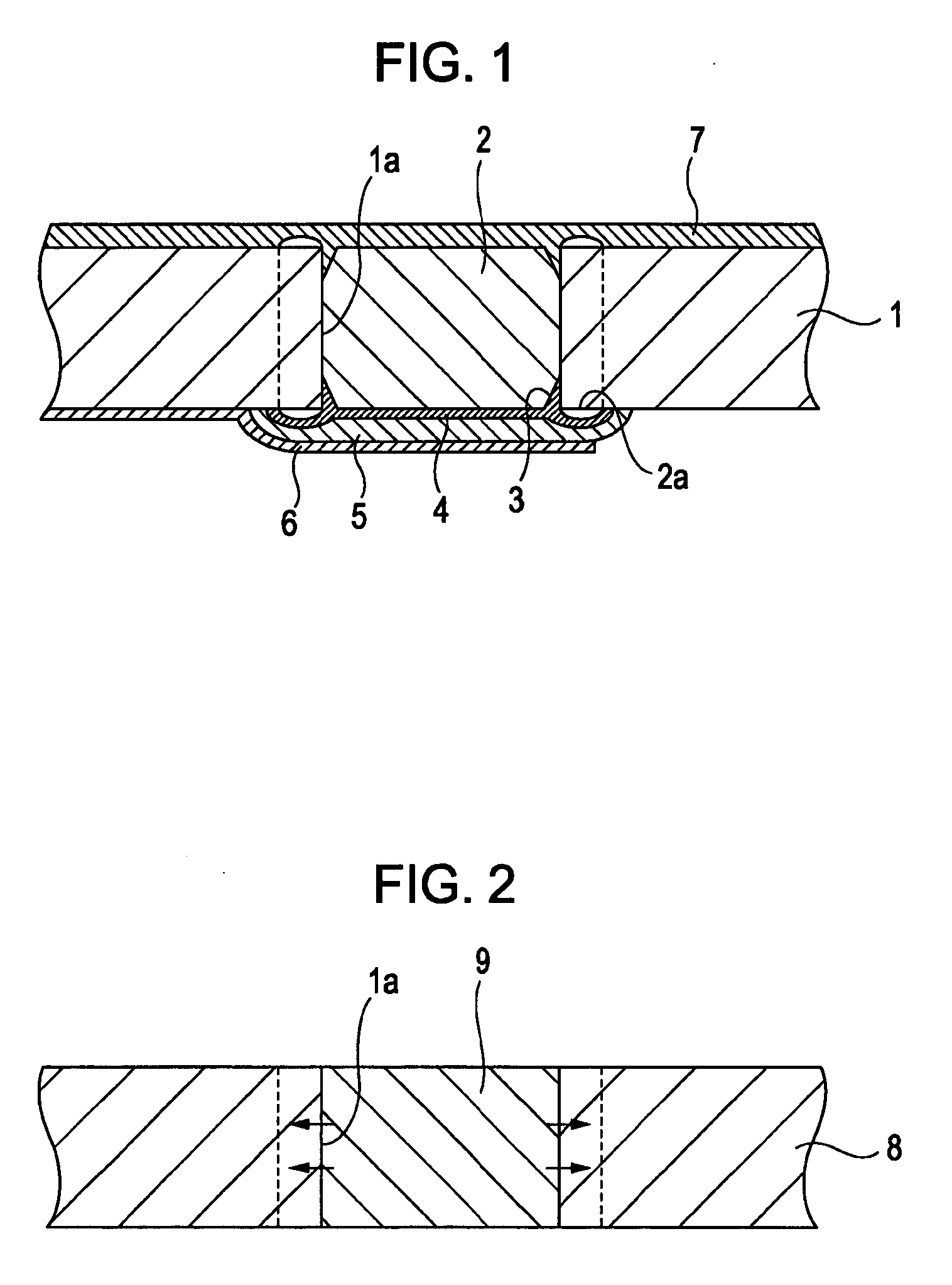
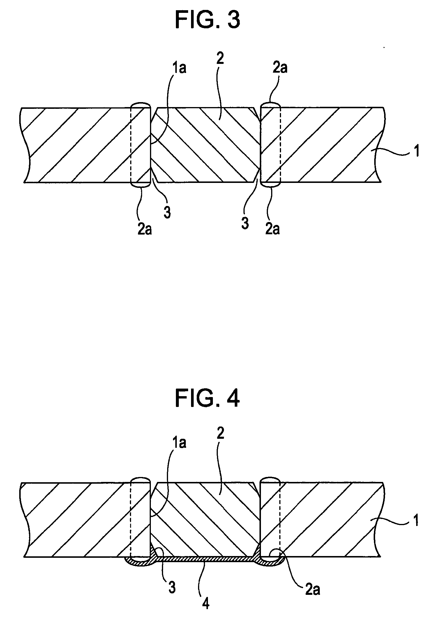
[0044]Embodiments of the present invention will now be described with reference to the accompanying drawings. FIG. 1 shows a principal part of a wiring board according to the present invention in cross section. FIG. 2 illustrates a first step of a method for manufacturing the wiring board according to the present invention. FIG. 3 illustrates a second step of the method. FIG. 4 illustrates a third step of the method. FIG. 5 illustrates a fourth step of the method. FIG. 6 illustrates a fifth step of the method.

[0045]The wiring board has a configuration as described below. With reference to FIG. 1, the wiring board includes a ceramic substrate 1 having a via-hole 1a, a via-conductor 2 disposed in the via-hole 1a, and a metal thin-film pattern 6. The ceramic substrate 1 is made of low-temperature co-fired ceramic (LTCC). The via-conductor 2 contains sliver or a material principally containing silver. A silver deposit 2a that is a piece of the via-conductor 2 is disposed on a surface po...


PUM

PropertyMeasurementUnit
Temperatureaaaaaaaaaa

Abstract

A wiring board in which silver is deposited near a via-conductor includes a ceramic substrate having a via-hole, a via-conductor disposed in the via-hole, and a metal thin-film pattern which is disposed on the ceramic substrate such that the metal thin-film pattern is connected to the via-conductor. The via-conductor contains silver or a material principally containing silver. A silver deposit that is a piece of the via-conductor is disposed on a surface portion of the ceramic substrate that is located near the via-hole. A catalyst layer containing a metal material is disposed over an exposed face of the via-conductor and the surface portion of the ceramic substrate. A metal layer is disposed on the catalyst layer. The metal thin-film pattern is disposed over the metal layer and the ceramic substrate.

Description

BACKGROUND OF THE INVENTION[0001]1. Field of the Invention[0002]The present invention relates to a wiring board suitable for various electric apparatuses and electronic circuit units and also relates to a method for manufacturing such a wiring board.[0003]2. Description of the Related Art[0004]A conventional wiring board and a method for manufacturing the wiring board will now be described with reference to the accompanying drawings. FIG. 7 shows a principal part of the conventional wiring board in cross section. FIG. 8 illustrates a first step of the method, FIG. 9 illustrates a second step of the method, FIG. 10 illustrates a third step of the method, and FIG. 11 illustrates a fourth step of the method.[0005]The conventional wiring board has a configuration as described below. With reference to FIG. 7, the conventional wiring board includes a ceramic substrate 51 having a via-hole 51a. The via-hole 51a accommodates a via-conductor 52.[0006]Since cavities 53 are formed in the ceram...

Claims


Application Information

Patent Timeline
IPC IPC(8): H05K7/00H05K1/18
CPCH05K3/246H05K3/4061H05K2201/0317Y10T29/49124H05K2201/09481H05K2203/0716H05K2203/072H05K2201/0347
Inventor TAKEUCHI, MASAYOSHIMURATA, SHINJI
Owner ALPS ALPINE CO LTD
Why Eureka
Try Eureka