Semiconductor power component and a method of producing same

Inactive Publication Date: 2005-09-27
ROBERT BOSCH GMBH
View PDF5 Cites 4 Cited by
  • Summary
  • Abstract
  • Description
  • Claims
  • Application Information

AI Technical Summary

Benefits of technology

[0025]It is an object of the present invention to provide a rugged IGBT for ignition applications in particular

Problems solved by technology

This is a highly complex procedure and has become possible only in recent years (see, for example, T. Laska et al., Conf. Proc. ISPSD '97, pages 361-364).
Such as buffer is feasible only to a limited extent in the production of crude wafers using such a double EPI/substrate wafer due to buffer outward diffusion.
Nevertheless, this operating case makes high demands on the pulse strength of IGBT 30′ due to the high energy conver

Method used


Image

  • Semiconductor power component and a method of producing same
  • Semiconductor power component and a method of producing same
  • Semiconductor power component and a method of producing same

Examples


Example

[0041]The same reference numbers in the figures denote the same components or those having the same function.

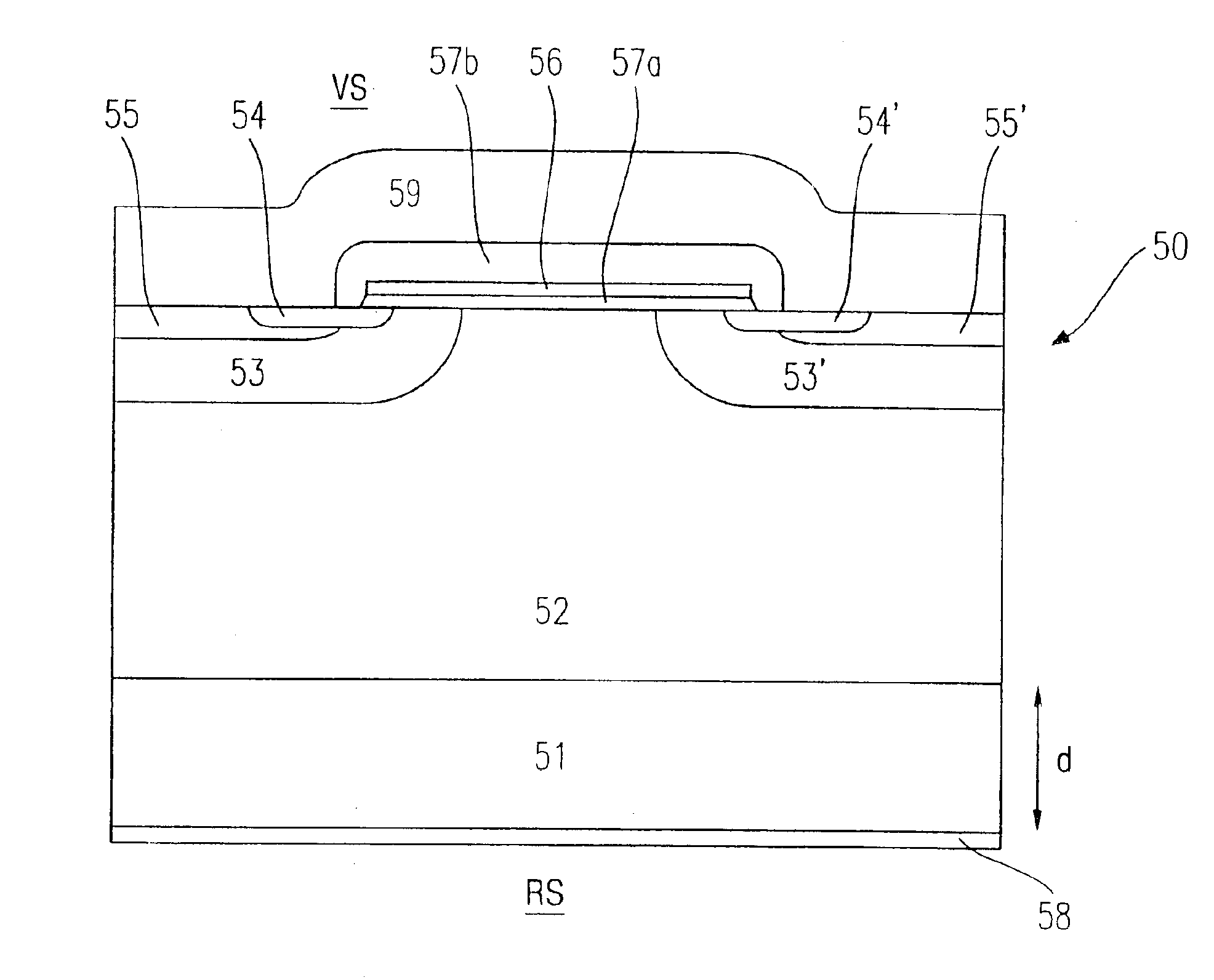
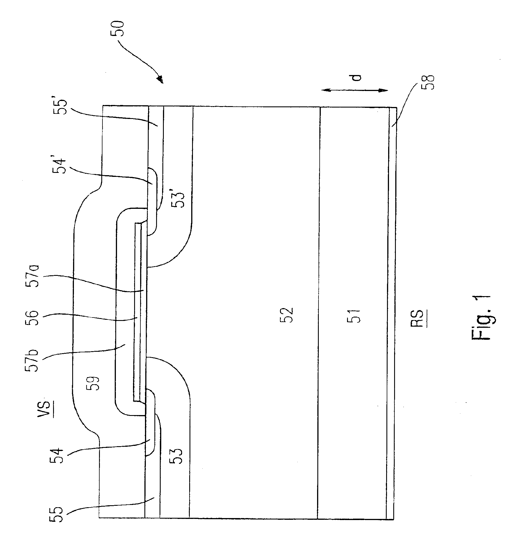
[0042]FIG. 1 shows a schematic cross-sectional diagram of a vertical NPT-IGBT according to exemplary embodiment of the present invention.

[0043]FIG. 1 shows an active region 50 of an NPT-IGBT and a corresponding n−p+ substrate 51, 52. This substrate 51, 52 is either an n− wafer substrate including a rear-side p+ diffusion or an n−p+ SDB crude wafer or an n− wafer substrate including a rear-side p+ epitaxy layer.

[0044]As mentioned above, n− drift region 52 in said n−p+ substrate is the known drift region in active region 50 of the IGBT, and p+ rear side 51 is the anode-side emitter.

[0045]FIG. 1 shows in particular a cross section through a cell and / or a strip within the active region of the IGBT without the passivation layers which are referred to in other systems. The entire active region may be obtained by monolithic integration of a plurality of such cells, i.e., strips side...


PUM


Abstract

A semiconductor power component and a method for producing a semiconductor power component, in particular a vertical NPT-IGBT for ignition applications with a breakdown voltage of less than approx. 1000 V. The semiconductor power component includes a wafer substrate of a first conductive type including a rear-side emitter region of a second conductive type and a front-side drift region of the first conductive type; a rear-side anode contact which is connected to the emitter region and extends partially to the front-side surface; a front-side MOS control structure; and a front-side cathode contact which is connected to a front-side source region and a body region of the front-side MOS control structure. The thickness of the drift region is much larger than the width of the space charge region at a defined breakdown voltage; and the thickness of the rear-side emitter region is greater than 5 μm.

Description

FIELD OF THE INVENTION[0001]The present invention relates to a semiconductor power component and a method of producing a semiconductor power component.BACKGROUND INFORMATION[0002]Although applicable to other similar semiconductor power components, the present invention and the problems on which it is based are described here with respect to a vertical IGBT (insulated gate bipolar transistor).[0003]In general, IGBTs are used as power circuit-breakers in a cutoff voltage range from a few hundred volts to a few thousand volts. In particular, the use of such IGBTs as an ignition transistor, i.e., as a switch on the primary side of an ignition coil, is of particular interest.[0004]The structure of a vertical IGBT resembles that of a VDMOS transistor, except that a p+ emitter is arranged on its anode side instead of an n+ substrate as in the VDMOS transistor. German Published Patent Application No. 31 10 230 discusses a vertical MOSFET component having the basic structure of a vertical IG...

Claims


Application Information

Patent Timeline
IPC IPC(8): H01L21/331H01L21/02H01L29/66H01L29/739
CPCH01L29/66333H01L29/7395
Inventor FLOHRS, PETERPLIKAT, ROBERTFEILER, WOLFGANG
Owner ROBERT BOSCH GMBH
Why Eureka
Try Eureka