High frequency module using metal-wall and method of manufacturing the same

a technology of high frequency modules and metal walls, applied in the direction of semiconductor devices, semiconductor/solid-state device details, electrical apparatus, etc., can solve the problems of insignificant shielding effect, degradation of performance and malfunction, and current flow to create electromagnetic noise, etc., to enhance the effect of shielding

Inactive Publication Date: 2007-10-25
SAMSUNG ELECTRO MECHANICS CO LTD
View PDF3 Cites 30 Cited by
  • Summary
  • Abstract
  • Description
  • Claims
  • Application Information

AI Technical Summary

Benefits of technology

[0015]The present invention has been made to solve the foregoing problems of the prior art and therefore an aspect of the present invention is to provide a compact high frequency module for enhancing effects of shielding an electromagnetic wave of a shielding metal film formed on a molding.
[0018]The metal wall is disposed on the substrate to spatially separate some of the surface mounted devices from the others. The metal wall has a bending depending on a mounting position of the surface mounted devices. Here, the metal wall has both ends extending to edges of the substrate, respectively. The metal wall disposed between the surface mounted devices serves to block interference from an electromagnetic wave radiated from the devices.
[0022]Preferably, the metal wall has a lightning rod structure with a planar main board and a plurality of fingers attached onto the planar main board. This structure enables a liquid molding material to flow in with minimal interference with the metal wall in a process of injecting the liquid molding material to form the molding.

Problems solved by technology

That is, regardless of the induction of the device, current flows to create electromagnetic noise, which is an unnecessary energy.
Such electromagnetic noise, if transferred to other devices through a path, leads to degradation in performance and malfunction thereof.
Yet, the metal film formed on the molding is not connected to a ground of the substrate, thus insignificant in terms of shielding effects.

Method used


Image

  • High frequency module using metal-wall and method of manufacturing the same
  • High frequency module using metal-wall and method of manufacturing the same
  • High frequency module using metal-wall and method of manufacturing the same

Examples


Embodiment Construction

[0036]Exemplary embodiments of the present invention will now be described in detail with reference to the accompanying drawings.

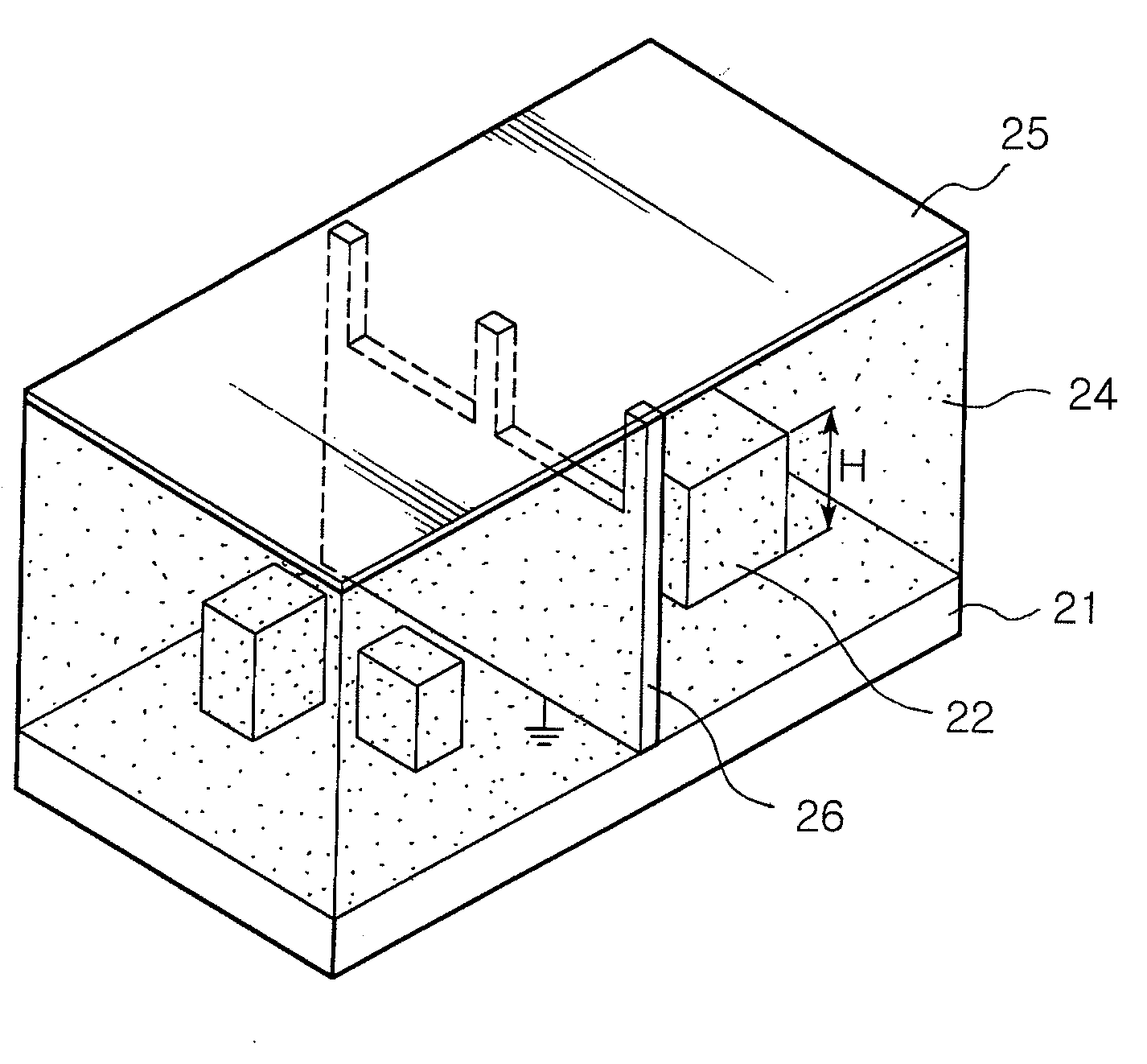
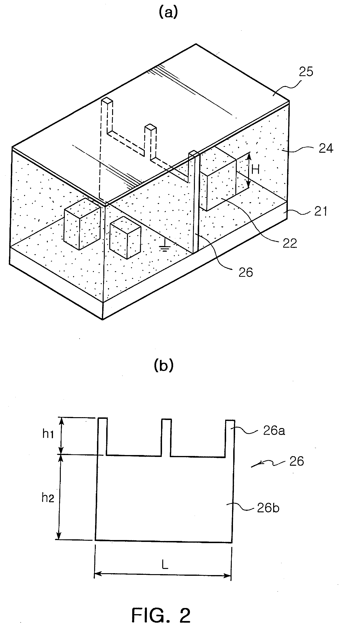
[0037]FIG. 2a is a perspective view illustrating a high frequency module using a metal wall according to an embodiment of the invention. FIG. 2b is a front elevation view illustrating the metal wall.

[0038]Referring to FIG. 2a, a substrate 21 is provided with semiconductor devices 22 and a metal wall 26 thereon. A metal film 25 is formed on a resin molding 24 sealing the devices 22 and the metal wall 26.

[0039]A ground (not illustrated) is formed inside or on a surface of the substrate.

[0040]The devices 22 mounted on the substrate 21 are connected to one another by a circuit (not illustrated) on the substrate 21, performing various functions.

[0041]Also, the resin molding 24 hermetically seals a high frequency device or electronic product, thereby improving moisture-resistant or impact-resistant characteristics over a conventional metal cap. Moreover, the met...


PUM

PropertyMeasurementUnit
thicknessaaaaaaaaaa
thicknessaaaaaaaaaa
frequencyaaaaaaaaaa

Abstract

A high frequency module and a manufacturing method thereof In the module, a substrate has a ground. A plurality of surface mounted devices are mounted on the substrate. A metal wall is connected to the ground of the substrate. A resin molding hermetically seals the surface mounted devices and the metal wall, the resin molding formed to expose a top surface of the metal wall. Also, a metal film is formed on the resin molding to contact the top surface of the exposed metal wall.

Description

CLAIM OF PRIORITY[0001]This application claims the benefit of Korean Patent Application No. 2006-36110 filed on Apr. 21, 2006 in the Korean Intellectual Property Office, the disclosure of which is incorporated herein by reference.BACKGROUND OF THE INVENTION[0002]1. Field of the Invention[0003]The present invention relates to a high frequency module and a manufacturing method thereof, and more particularly, to a high frequency module in which a metal shielding film is grounded by a metal wall in forming a shielding structure of the high frequency module, and a manufacturing method thereof.[0004]2. Description of the Related Art[0005]A high frequency module for use in a mobile telecommunication device such as a mobile phone is constructed of a high frequency circuit including a high frequency semiconductor device and a periphery circuit that are formed on a substrate thereof.[0006]In general, current propagating in an electronic device induces electric field and magnetic field therear...

Claims


Application Information

Patent Timeline
Patent Type & Authority Applications(United States)
IPC IPC(8): H01L23/34
CPCH01L23/3121H01L23/552H01L23/66H01L25/165H01L2924/3025H01L2924/0002H05K9/003H05K9/0032H01L2924/00H05K9/0024H05K9/00
Inventor OH, KWANG JAESUNG, JE HONGCHOI, YOON HYUCKLEE, TAE SOO
Owner SAMSUNG ELECTRO MECHANICS CO LTD
Why Eureka
Try Eureka