Method for manufacturing stacked package structure

a technology of stacked package and packaging structure, which is applied in the direction of basic electric elements, electrical equipment, semiconductor devices, etc., can solve the problems of substantial increase in cost, serious deterioration of stacked package structure, and greatly reduced yield of stacked package process, so as to reduce the area occupied by the package structure and reduce the area of the printed circuit board

Inactive Publication Date: 2007-11-01
ADVANCED SEMICON ENG INC
View PDF0 Cites 102 Cited by
  • Summary
  • Abstract
  • Description
  • Claims
  • Application Information

AI Technical Summary

Benefits of technology

[0008] Therefore, one objective of the present invention is to provide a method for manufacturing a stacked package structure, which can reduce the area occupied by the package structure to greatly decrease the area of a printed circuit board.
[0009] Another objective of the present invention is to provide a method for manufacturing a stacked package structure, which can integrate the connection between an upper chip package structure and a bottom chip package structure.
[0010] Still another objective of the present invention is to provide a method for manufacturing a stacked package structure, which can effectively avoid warpage from occurring in the connection of chip package structures, and prevent a cold joint condition from occurring between the chip package structures, so as to greatly enhance the yield of the stacked package structure.

Problems solved by technology

As a result, the reliability of the stacked package structure is seriously deteriorated, the yield of the package process is greatly reduced, and the cost is substantially increased.

Method used


Image

  • Method for manufacturing stacked package structure
  • Method for manufacturing stacked package structure
  • Method for manufacturing stacked package structure

Examples


Embodiment Construction

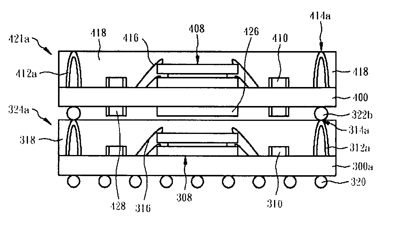
[0021] The present invention discloses a stacked package structure and a method for manufacturing the same. In order to make the illustration of the present invention more explicit and complete, the following description is stated with reference to FIGS. 4 to 12c.

[0022] Referring to FIGS. 4 to 9b and FIG. 12a, in which FIGS. 4 to 9b are schematic flow diagrams showing the process for manufacturing a stacked package structure in accordance with a first preferred embodiment of the present invention. In the fabrication of a stacked package structure of the present invention, a chip package structure 324a, such as illustrated in FIG. 8, is typically formed firstly. In the formation of the chip package structure 324a, a substrate 300a or a substrate 300b is provided, in which the substrate 300a or the substrate 300b may be a printed circuit board, for example. Alternatively, the substrate 300a or 300b can be replaced by other chip carrier, such as a QFP leadframe or a QFN leadframe. The...


PUM


Abstract

A method for manufacturing a stacked package structure is disclosed, comprising: forming a first chip package structure, comprising: providing a chip carrier having a first and a second surface in opposition to each other; forming bonding wires on the first surface; providing at least one chip on and electrically connected to the first surface; and forming an encapsulant covering the first surface, the chip and the bonding wires, wherein a top end of each bonding wire is exposed at a surface of the encapsulant; forming a plurality of electrical connections respectively deposed on the top end of each bonding wire; and providing a second chip structure electrically jointed with the electrical connections and stacked on the first chip package structure.

Description

CROSS-REFERENCE TO RELATED APPLICATIONS [0001] This application is a continuation-in-part of U.S. application Ser. No. 11 / 409,933, filed on Apr. 24, 2006, hereby incorporated by reference as it fully set forth herein.FIELD OF THE INVENTION [0002] The present invention relates to a system-in-package (SiP) structure and a method for manufacturing the same, and more particularly, to a stacked package structure and a method for manufacturing the same. BACKGROUND OF THE INVENTION [0003] The demand for low cost, small size, and more functionality has become the main driving force in the electronic industry. To achieve such goals, advanced packaging techniques like flip chip, chip scale package, wafer level packaging, and 3D packages have been developed. The 3D packaging technique is developed to integrate dies, packages and passive components into one package, in other words, to achieve system in a package solution. The integration can be made in side-by-side, stacked, or both manners. Th...

Claims


Application Information

Patent Timeline
Patent Type & Authority Applications(United States)
IPC IPC(8): H01L21/00
CPCH01L25/0657H01L25/105H01L2224/73265H01L2224/32225H01L2224/32145H01L2225/1058H01L2225/1023H01L2924/3511H01L2924/19107H01L2924/19106H01L2924/19105H01L2924/19041H01L2924/15331H01L2924/15311H01L2924/01079H01L2924/01078H01L25/16H01L2224/48091H01L2224/48227H01L2225/0651H01L2225/06589H01L2225/1052H01L2924/00014H01L2924/00012H01L2924/00H01L2924/181H01L24/73
Inventor LEE, YONGGILL
Owner ADVANCED SEMICON ENG INC
Why Eureka
Try Eureka