

Display substrate, method of manufacturing the same and display apparatus having the same
- Summary
- Abstract
- Description
- Claims
- Application Information
AI Technical Summary
Benefits of technology
Problems solved by technology
Method used
Image

Examples
Embodiment Construction
[0018]Exemplary embodiments of the invention are described more fully hereinafter with reference to the accompanying drawings. This invention may, however, be embodied in many different forms and should not be construed as limited to the exemplary embodiments set forth herein.
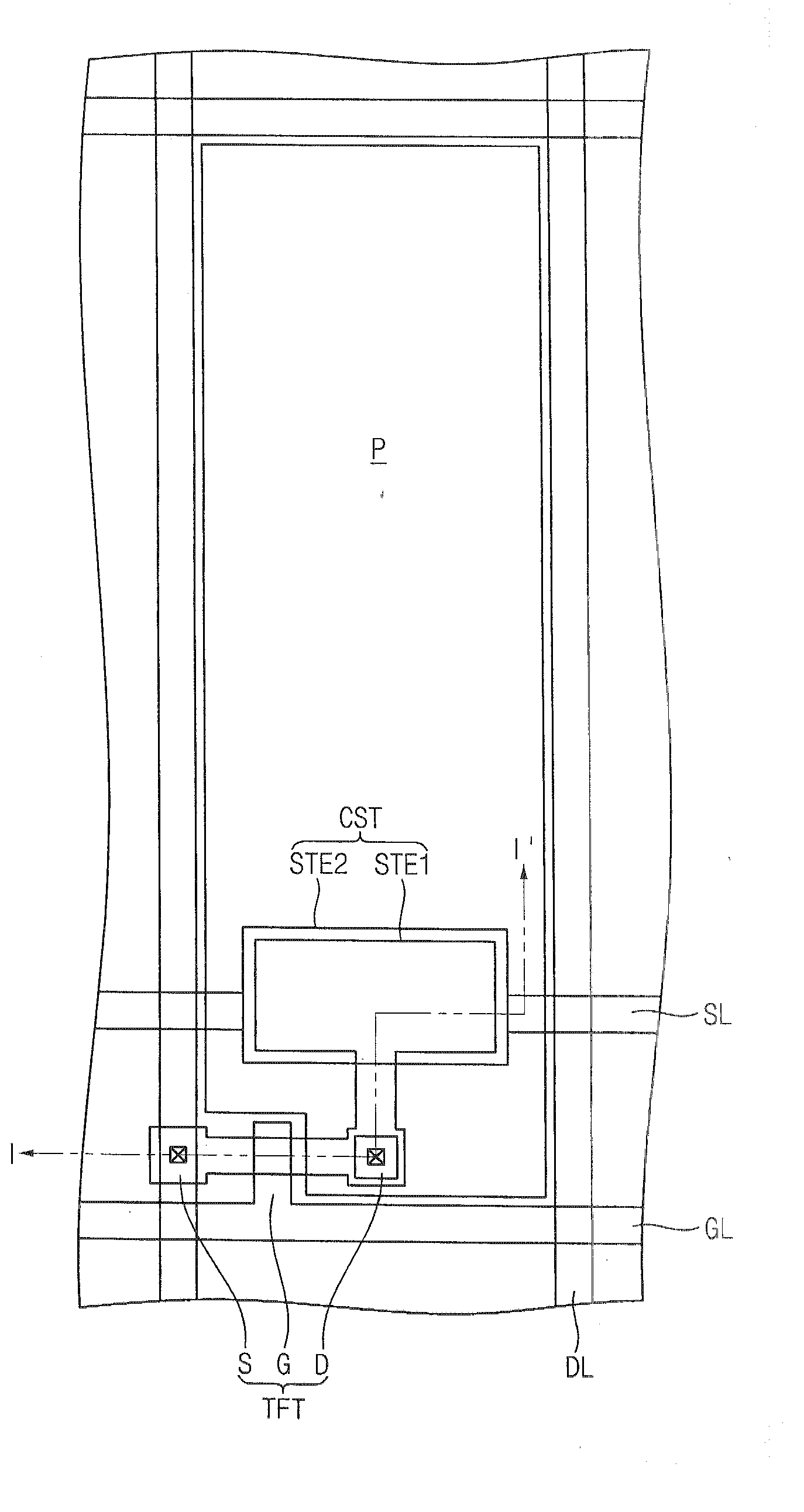
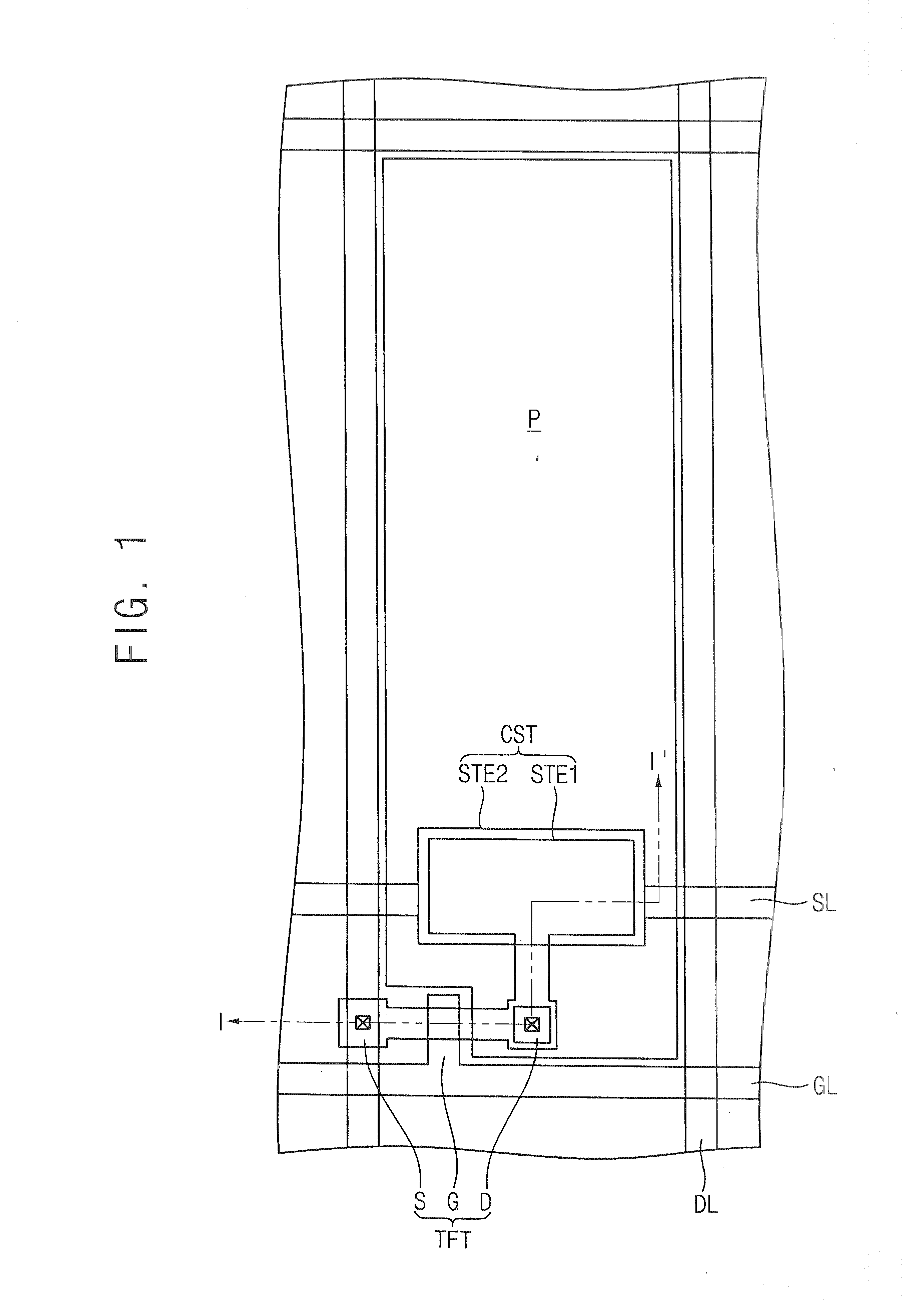
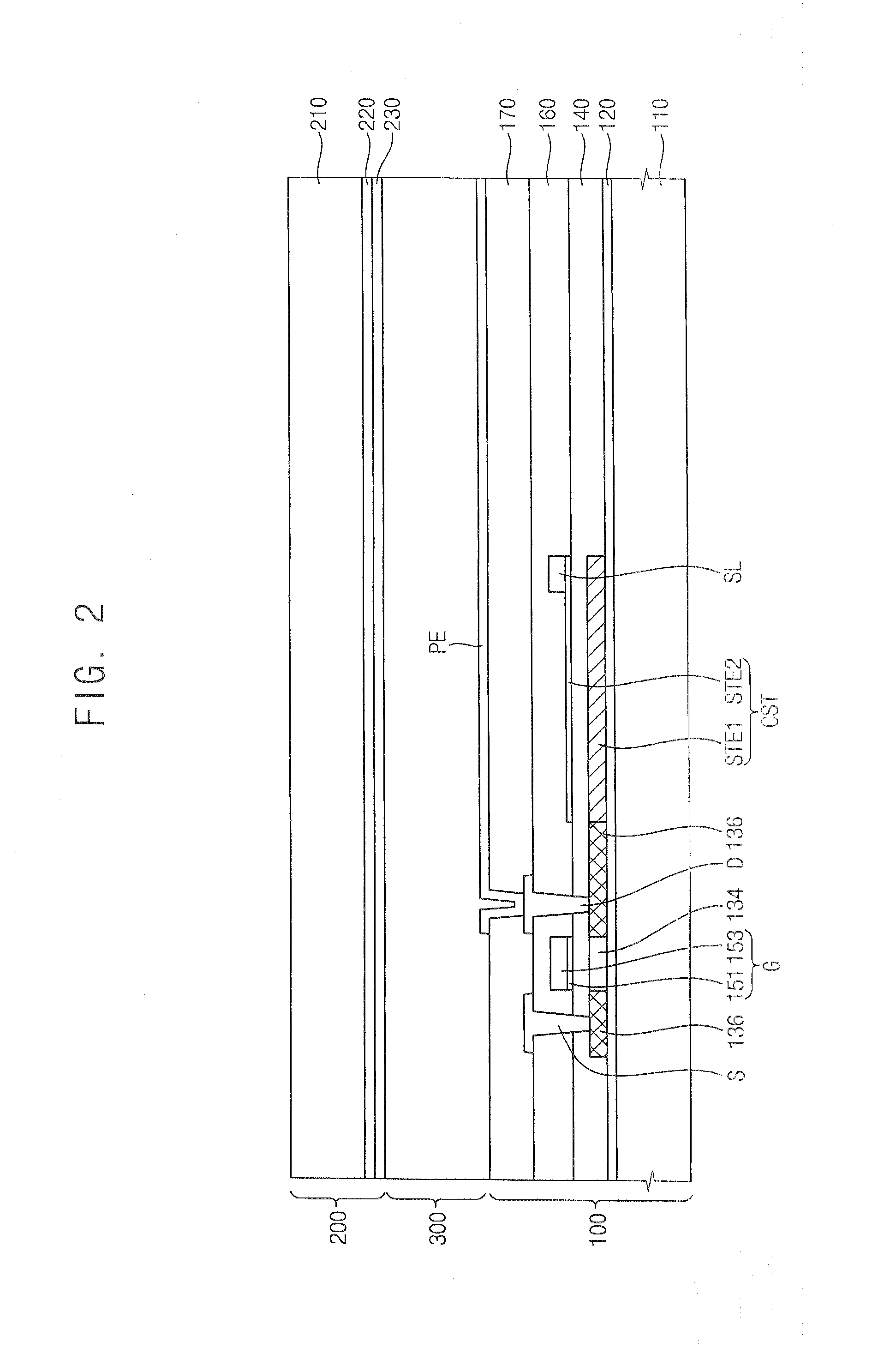
[0019]FIG. 1 is a plan view illustrating a display apparatus according to an exemplary embodiment of the present invention. FIG. 2 is a cross-sectional view taken along a line I-I′ in FIG. 1.
[0020]Referring to FIGS. 1 and 2, a display apparatus includes a display substrate 100 and an opposite substrate 200 that faces the display substrate 100 and a liquid crystal layer 300 interposed between the display substrate 100 and the opposite substrate 200. The display substrate 100 includes a first base substrate 110 and a plurality of pixels P that is formed on the first base substrate 110 and is arranged in a matrix. A pixel electrode PE is formed in each of the pixels P. The opposite substrate 200 includes a second ...
PUM
 Abstract
Description
Claims
Application Information