Method for fabricating semiconductor device

a semiconductor device and manufacturing method technology, applied in semiconductor/solid-state device manufacturing, basic electric elements, electric devices, etc., can solve the problems of signal delay, signal delay, signal transfer delay through wiring, etc., to achieve high-reliability wiring, prevent the oxidation of the entire seed film into copper oxide, and high-reliability wiring

Inactive Publication Date: 2007-11-15
PANASONIC CORP
View PDF5 Cites 0 Cited by
  • Summary
  • Abstract
  • Description
  • Claims
  • Application Information

AI Technical Summary

Benefits of technology

[0017]The present invention is proposed in view of the above circumstances and has as its objective to provide a method of fabricating a semiconductor device in which defective filling due to disappearance of the seed film is prevented and highly reliable wiring is ensured.
[0021]With the above configuration, the oxidization of the first conductive film before the electrolytic plating for forming the second conductive film is started after the completion of the first conductive film is prevented. Therefore, the appearance of a void at the bottom of the recesses during the formation of the second conductive film can be prevented and highly reliable wiring is formed.
[0022]With the present invention, the oxidization of the entire seed film into copper oxide is prevented when a thin copper film is formed as the seed film in the recesses in the interlayer insulating film. No area is found in the recesses where the seed film dissolves and disappears when the semiconductor substrate on which the seed film is formed is immersed in a plating solution for forming a copper-plating film by electrolytic plating using the seed film as an electrode. A copper-plating film can be formed in the recesses without any void. Consequently, a semiconductor device with highly reliable wiring can be fabricated.

Problems solved by technology

In such semiconductor devices, signal delay is a factor in restricting the operation speed of the semiconductor devices.
Signal delay predominantly results from delay of signals transferred through wiring, namely wiring delay.
However, copper is easily oxidized.
Moreover, because of the difficulty in etching copper, the damascene process is used to form multilayer wiring.

Method used


Image

  • Method for fabricating semiconductor device
  • Method for fabricating semiconductor device
  • Method for fabricating semiconductor device

Examples


Embodiment Construction

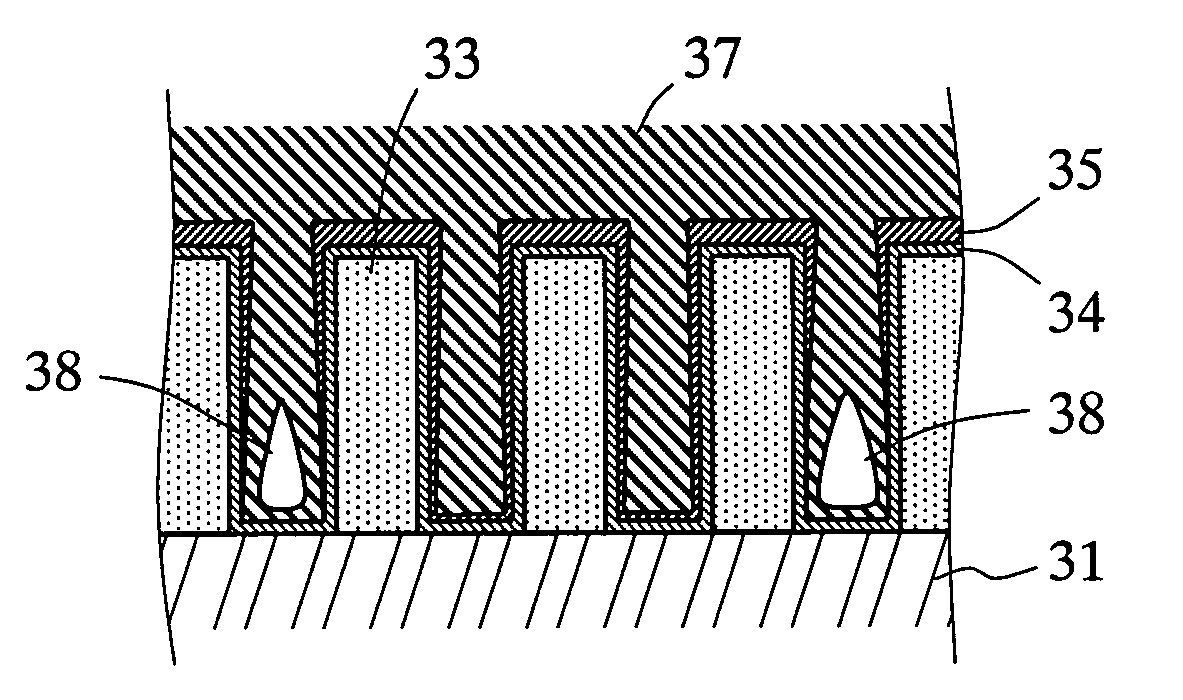
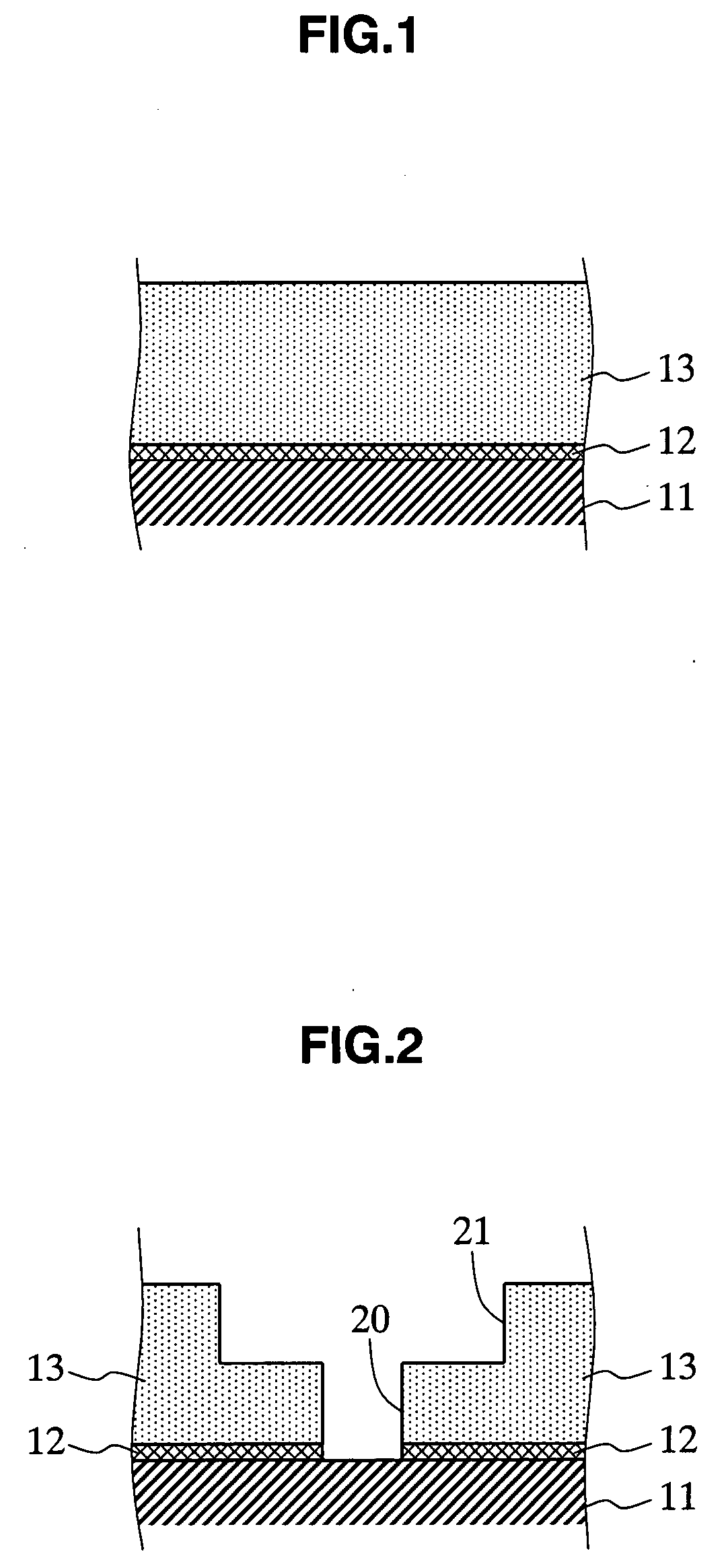
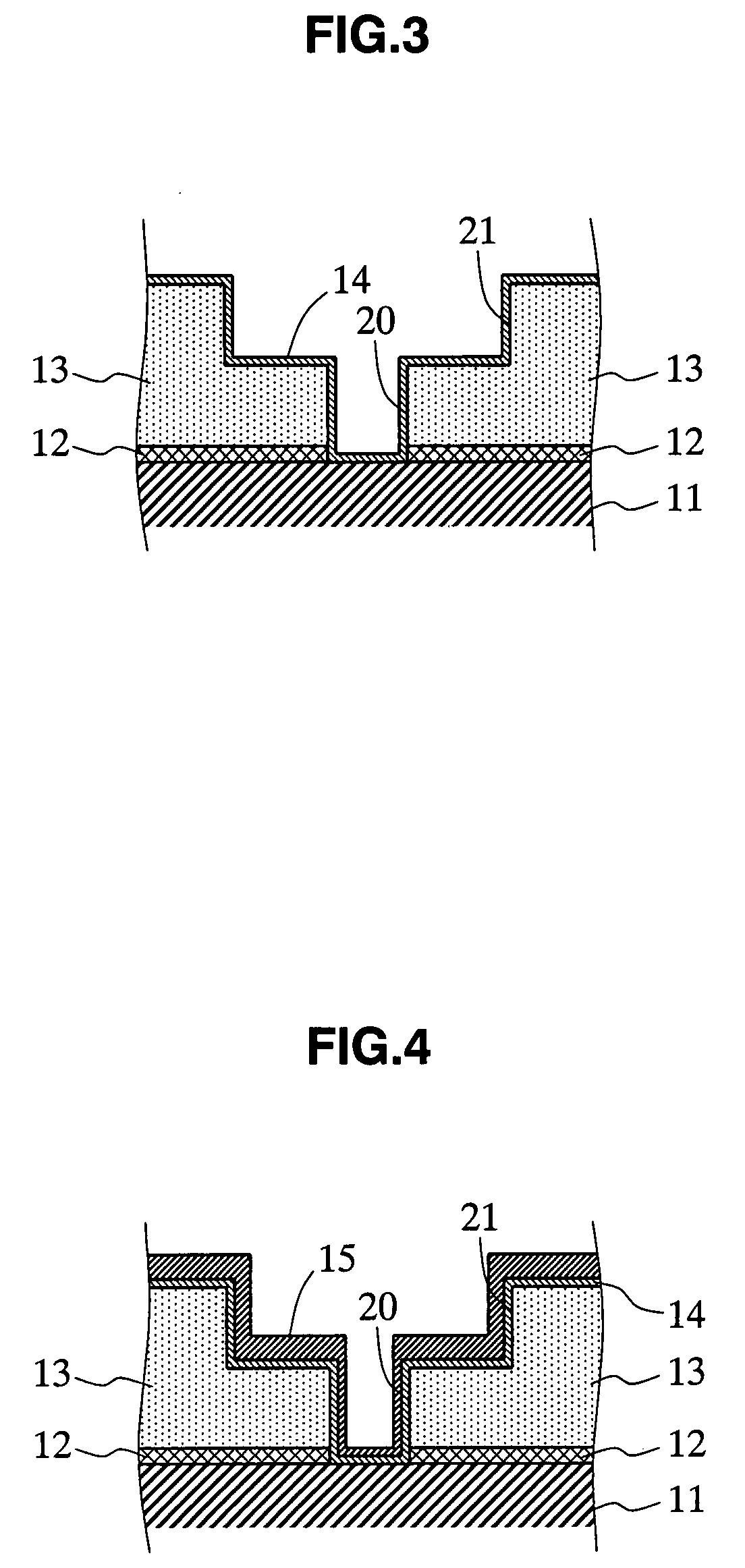
[0036]An embodiment of the method of fabricating a semiconductor device according to the present invention is described in detail hereafter with reference to the drawings. In the embodiment, the present invention is realized in a method of fabricating a semiconductor device by the dual damascene technique. FIGS. 1 to 8 are cross-sectional views showing the fabrication process of a semiconductor device having a multilayer wiring structure. In FIGS. 1 to 8, a semiconductor substrate on which semiconductor elements such as transistors and other wiring are formed is present below a lower wiring 11. However, the structure below the lower wiring 11 is not directly relevant to the present invention and, therefore, its explanation is omitted.

[0037]As shown in FIG. 1, first, an anti-diffusion barrier film 12 such as a carbon-added insulating film and a silicon nitride film is formed on the, for example copper, lower wiring 11 in the method of fabricating a semiconductor device of this embodi...


PUM


Abstract

The method of fabricating a semiconductor device according to the present invention is applied to a semiconductor device fabricated by forming a seed film in recesses formed in an interlayer film and forming a thick film embedded in the recesses by electrolytic plating using the seed film as an electrode. In this fabrication method, the maximum length of time until the electrolytic plating is started after the completion of the seed film is limited based on the formation of the seed film in the recesses. The maximum time is reduced as the recesses have higher aspect ratios, preventing a void from being formed in the recesses during the plating, thereby obtaining highly reliable wiring.

Description

CROSS-REFERENCE TO RELATED APPLICATION[0001]The present application claims the benefit of patent application number 2006-129861, filed in Japan on May 9, 2006, the subject matter of which is incorporated herein by reference.BACKGROUND OF THE INVENTION[0002]1. Field of the Invention[0003]The present invention relates to a method for fabricating a semiconductor device and particularly relates to fabrication of wirings used in a semiconductor device.[0004]2. Description of the Related Art[0005]Multilayer wiring structures are extensively used and wire intervals in a wiring layer become smaller as semiconductor devices become smaller (more highly integrated). In such semiconductor devices, signal delay is a factor in restricting the operation speed of the semiconductor devices. Signal delay predominantly results from delay of signals transferred through wiring, namely wiring delay. The wiring delay is presented by the product of inter-wiring capacity and wiring resistance (time constant...

Claims


Application Information

Patent Timeline
Patent Type & Authority Applications(United States)
IPC IPC(8): H01L21/44
CPCH01L21/76877H01L21/76873H01L21/3205
Inventor TAKAMORI, YOSHINORIBABA, NAOYUKIAOKI, NORISHIGE
Owner PANASONIC CORP
Why Eureka
Try Eureka