Layout compiler

a layout compiler and compiler technology, applied in semiconductor/solid-state device testing/measurement, instruments, measurement devices, etc., can solve problems such as inflexibleness, inability to easily reuse layouts in a given design, and easy errors in drawing shapes comprising layouts

Inactive Publication Date: 2007-11-22
PDF SOLUTIONS INC
View PDF4 Cites 10 Cited by
  • Summary
  • Abstract
  • Description
  • Claims
  • Application Information

AI Technical Summary

Benefits of technology

[0007]Aspects of an exemplary method for creating layouts for semiconductor test structures, as presented herein, include creating a first cell, and drawing one or more objects in the first cell. The one or more objects represent shapes of features for a semiconductor test structure. The method also includes, after drawing the one or more objects in the first cell, defining one or more parameters for each of the one or more objects drawn in the first cell. In a particular example, the method includes defining a test structure layout using a tree of cells that includes one or more instances of the first cell, and creating machine readable code using the tree of cells. Thereafter, the machine readable code may be executed with different values for the one or more parameters of the one or more objects drawn in the first cell to generate a set of different test structure layouts.

Problems solved by technology

However, drawing shapes comprising a layout is a process easily prone to errors.
Additionally, PCELLS lacks a capability to easily reuse layout in a given design.
Writing SKILL™ code to specify a pcell is also error prone and not flexible enough to realistically implement either large designs or to allow easy modification and maintenance of layout created with the code.
Such approaches also do not generally provide, to the degree desired, ease of design, portability, and ease of maintenance of layouts created with those approaches.

Method used


Image

  • Layout compiler
  • Layout compiler
  • Layout compiler

Examples


Embodiment Construction

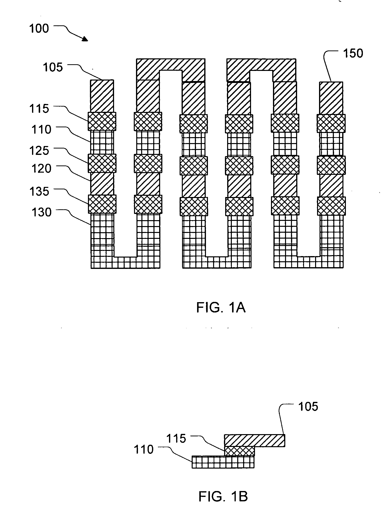
[0028]FIG. 1A illustrates a top view of layout for a via chain 100. Via chain 100 comprises a connector 105 in a top metal layer, connected by via 115 to a metal run 110 in a lower metal layer. Metal run 110 in turn is connected to a metal run 120 in the top metal layer through via 125. In turn, metal run 120 connects with metal run 130 through via 135. Ultimately, via chain 100 terminates at connector 150. Thus, via chain 100 is, when formed on a semiconductor wafer, an interconnected series of metal lines running through two separate layers of metal (other via chains can include metal runs in more than two layers), where those layers are connected by vias.

[0029]As such, via chain 100 allows a process to be tested and examined for via alignment with metal layers, for example. This testing may proceed by applying a voltage across connector 105 and connector 150 and measuring a current flow through via chain 100. Variations in current from what is expected may be indicative of alignm...


PUM


Abstract

For methods of creating pluralities of semiconductor test structure layouts from a graphical specification, systems include a GUI to draw objects representing shapes of such layout, and to parameterize those objects to size and interrelate those objects. The GUI supports placement of cells in hierarchical layers. The graphical specification is parsed into an ASCII descriptor file from which node information is extracted and connection information among nodes preserved in separate graphs for an X direction and a Y direction of the layout. That node and connection information is further processed to obtain equations having variables (parameters) that relate points in the layout a defined point, and those equations used in forming source code that can be executed with values for the variables in the source code.

Description

BACKGROUND[0001]1. Field[0002]The present application relates to graphical specification of semiconductor structures, and, more particularly, to graphically specifying and parameterizing and automating layout generation for semiconductor test structures.[0003]2. Related Art[0004]Circuits formed with semiconductors structures may be fabricated using, for example, a lithography process involving masks that specify geometric designs that should be created at each layer of a plurality of layers in the semiconductor structures. Together, the masks specify a layout for the semiconductor structures for a particular circuit. The layout may comprise a number of shapes connected and arranged with respect to each other at a number of different layers. The connection and arrangement of theses shapes and the layers at which these shapes are disposed define the electrical function of one or more circuits implemented in the layout. Layout for a particular circuit is typically process dependent. De...

Claims


Application Information

Patent Timeline
Patent Type & Authority Applications(United States)
IPC IPC(8): G11C5/02
CPCG01R31/31707H01L22/34G11C5/025G01R31/318314
Inventor WEILAND, LARG H.DRAPATZ, STEFANDECKER, MARKUS R.
Owner PDF SOLUTIONS INC
Why Eureka
Try Eureka