Method and apparatus providing dark current reduction in an active pixel sensor

a technology of active pixel sensor and dark current reduction, which is applied in the field of semiconductor devices, can solve the problems of generating dark current, generating dark current, and generating conventional photo gates and photodiodes that do not perfectly generate charge in response to incident light,

Inactive Publication Date: 2007-11-29
MICRON TECH INC
View PDF13 Cites 84 Cited by
  • Summary
  • Abstract
  • Description
  • Claims
  • Application Information

AI Technical Summary

Problems solved by technology

Conventional photo gates and photodiodes do not, however, perfectly generate charge in response to incident light.
Dark current is perceived as noise in the pixel output signal.
Dark current is caused, in part, by defects in silicon, such as bulk defects, interface defects and surface defects.
Defects near the surface are particularly susceptible to exterior radiation sources and hence prone to generating dark current.
In either case, the dark current generated at the site of holding of the generated charge is of primary concern because generated dark current is added to the held charge during the entire time that the charge is held, and the charge may be held for a relatively long period of time.
Thus, dark current generated in the storage node is more problematic than dark current generated in the photosensitive region during the integration time.
However, such solutions inevitably result in some loss of functionality of the active pixel sensor.

Method used


Image

  • Method and apparatus providing dark current reduction in an active pixel sensor
  • Method and apparatus providing dark current reduction in an active pixel sensor
  • Method and apparatus providing dark current reduction in an active pixel sensor

Examples


Embodiment Construction

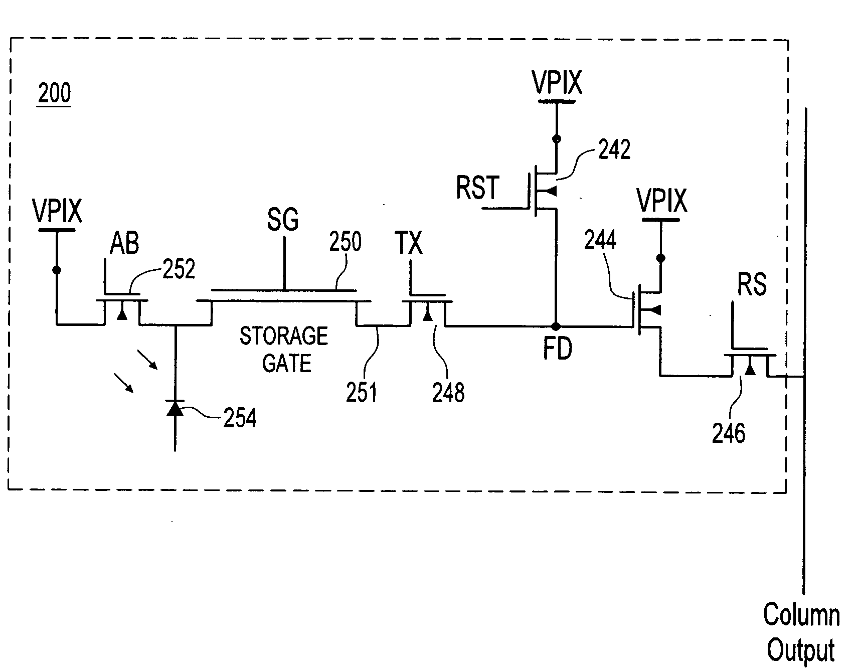
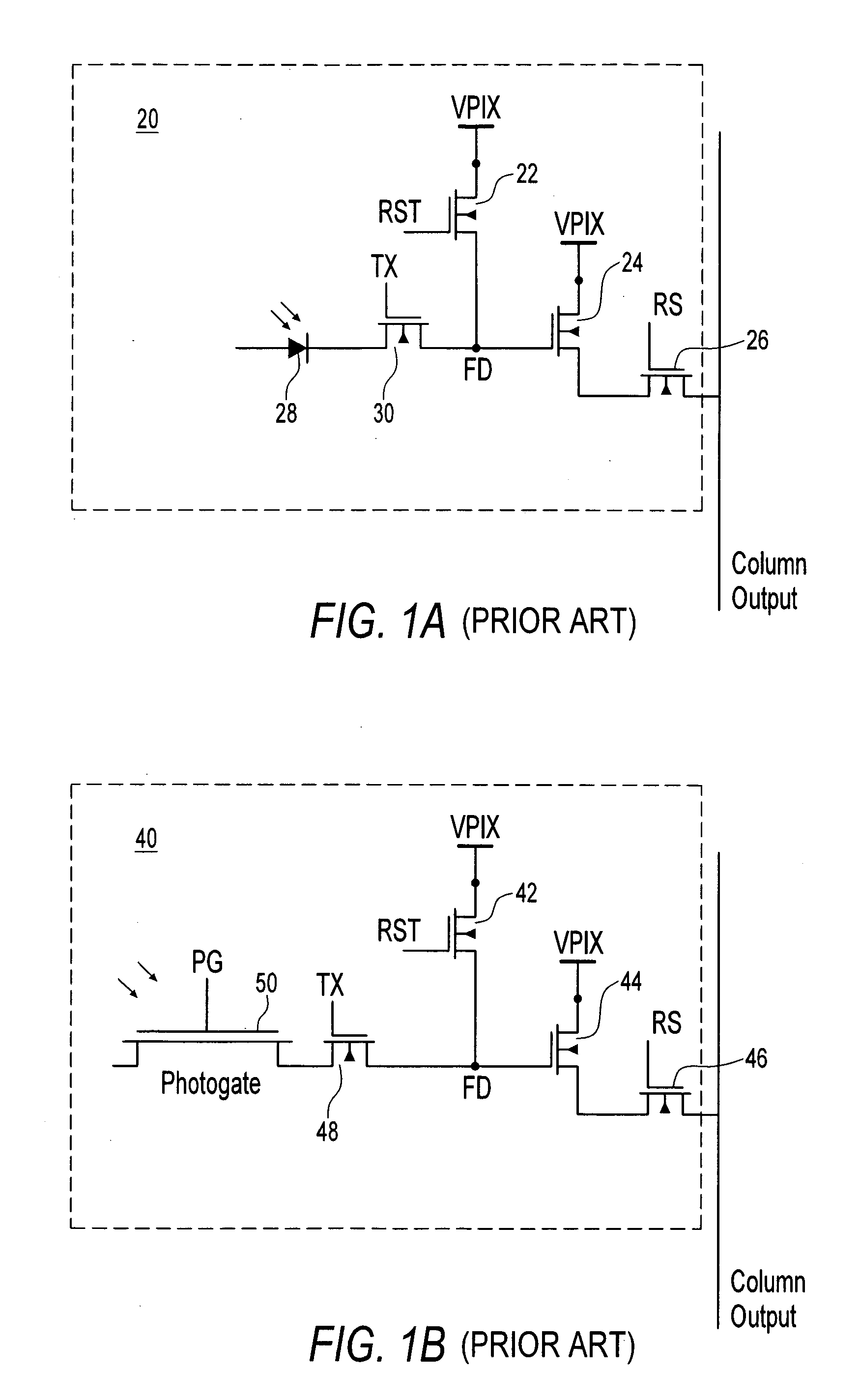
[0021]As described above, surface and interface-generated dark current result from defects in the silicon layers of a photodetector (e.g., photodiode or photo gate) or in other storage areas of a pixel.

[0022]The surface defects in a pixel circuit facilitate the separation of electrons from holes near the surface of a semiconductor substrate, e.g., a silicon substrate, both in the photosensitive region and in a holding region. The free electrons generally travel to an n-type region of the pixel without recombining with holes. However, if the surface regions of the pixel were to include more holes than electrons, then many, even a majority of the electrons at the surface region could be recombined with holes before entering a charge collecting n-type region. The invention provides a method and structure for increasing recombination of electrons and holes in areas of a pixel which are subject to generation of dark current as explained below.

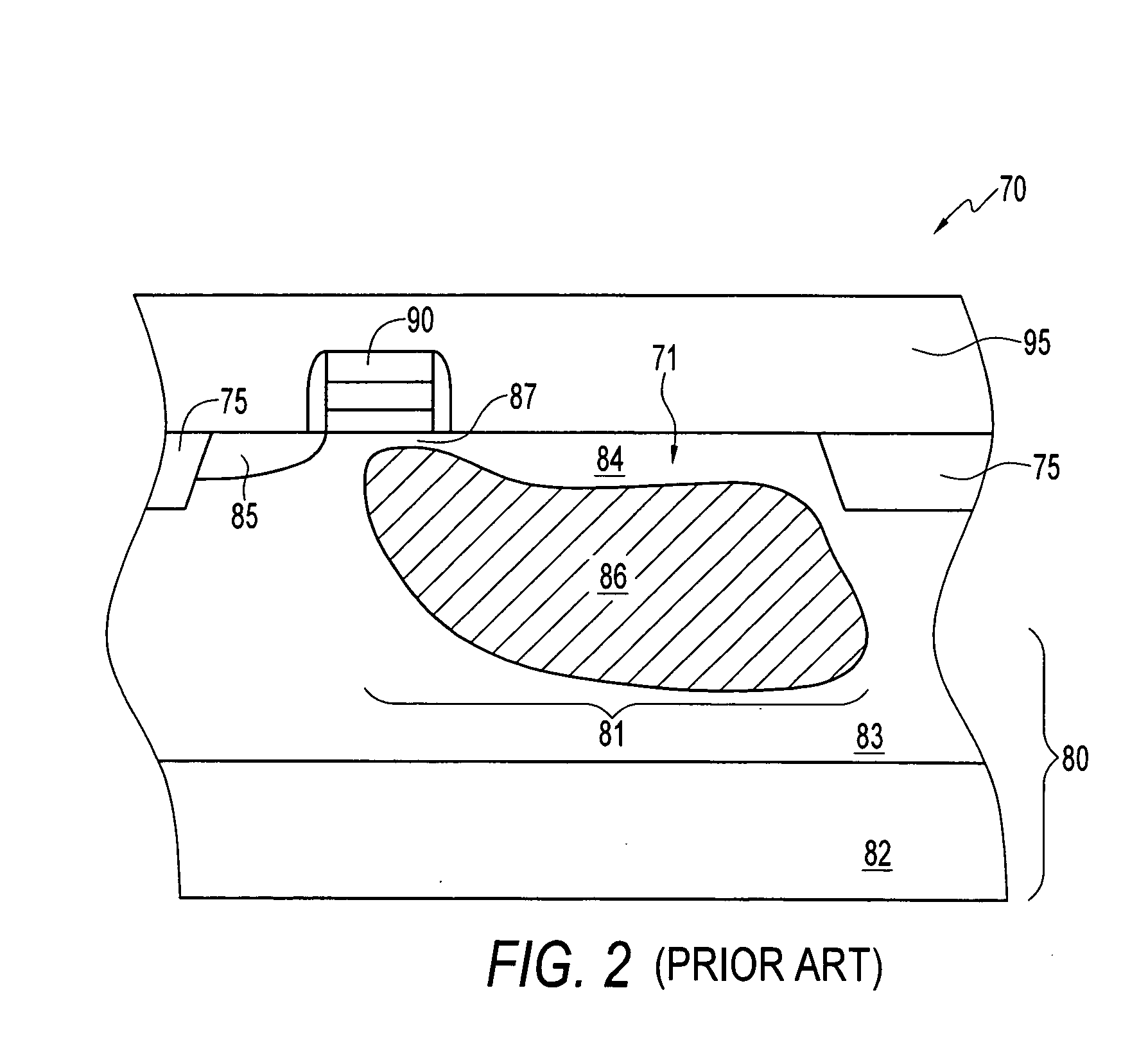
[0023]FIG. 3A shows the potentials of the val...


PUM


Abstract

An imager has one or more pixel circuits arranged to receive negatively biased control signals at one or more gates associated with charge holding regions to reduce dark current generation and flow.

Description

FIELD OF THE INVENTION[0001]The invention relates generally to semiconductor devices, and more specifically to dark current reduction in an imaging device.BACKGROUND OF THE INVENTION[0002]Optical communication and imaging systems generally require the conversion of light energy into electrical signals. The conversion of light energy to electrical signals involves the use of optical-to-electrical conversion circuits. An example of an optical-to-electrical conversion circuit is a complementary metal oxide semiconductor (“CMOS”) active pixel sensor circuit. Various active pixel sensor architectures are currently used, including photodiode and photo gate architectures. A photodiode active pixel sensor uses a photodiode, a reverse biased p-n junction, to produce an electrical signal that corresponds to the amount and type of light energy incident on the photodiode. Similarly, a photo gate active pixel sensor uses a capacitance formed by a capacitor, such as, for example, a polysilicon-ox...

Claims


Application Information

Patent Timeline
Patent Type & Authority Applications(United States)
IPC IPC(8): H01L27/00H04N5/225H04N5/361H04N5/369
CPCH01L27/14609H04N5/37452H04N5/361H04N25/63H04N25/771
Inventor XU, CHEN
Owner MICRON TECH INC
Why Eureka
Try Eureka