Interconnect structure and formation for package stacking of molded plastic area array package

a technology of interconnection structure and stacked packages, which is applied in the direction of semiconductor devices, semiconductor/solid-state device details, electrical equipment, etc., can solve the problem that conventional ball grid array (bga) packages do not allow interconnection between stacked packages

Active Publication Date: 2007-11-29
AVAGO TECH WIRELESS IP SINGAPORE PTE
View PDF99 Cites 254 Cited by
  • Summary
  • Abstract
  • Description
  • Claims
  • Application Information

AI Technical Summary

Problems solved by technology

Conventional ball grid array (BGA) packages do not allow for interconnection between stacked packages through the encapsulating material.

Method used


Image

  • Interconnect structure and formation for package stacking of molded plastic area array package
  • Interconnect structure and formation for package stacking of molded plastic area array package
  • Interconnect structure and formation for package stacking of molded plastic area array package

Examples


example advantages

[0079]Embodiments of the present invention provide many advantages over conventional BGA packages, including those described above with respect to FIGS. 1-4. Some of these advantages are described below. Each advantage described below does not necessarily apply to each embodiment described herein. Furthermore, the advantages provided by embodiments of the present invention are not necessarily limited to those described below.

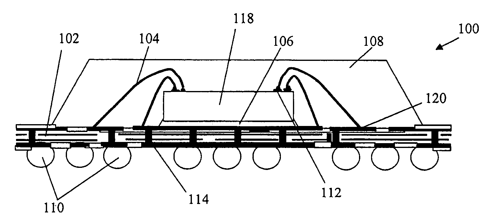
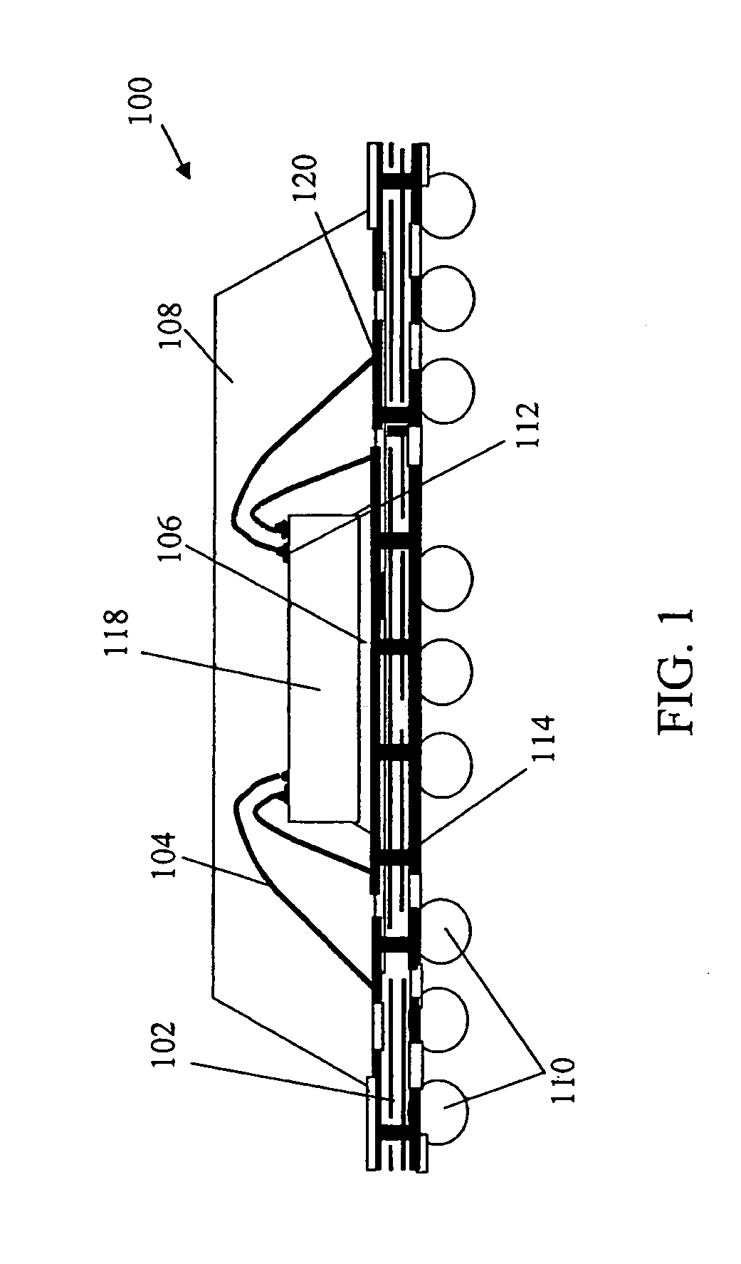
[0080](1) Packages according to embodiments of the present invention allow the mold encapsulation layer of the bottom package to span the entire surface of the substrate and allow the size of the IC package not to be limited by the size of the mold chase. Package footprint size for the bottom package can also be minimized for a given IC die size.

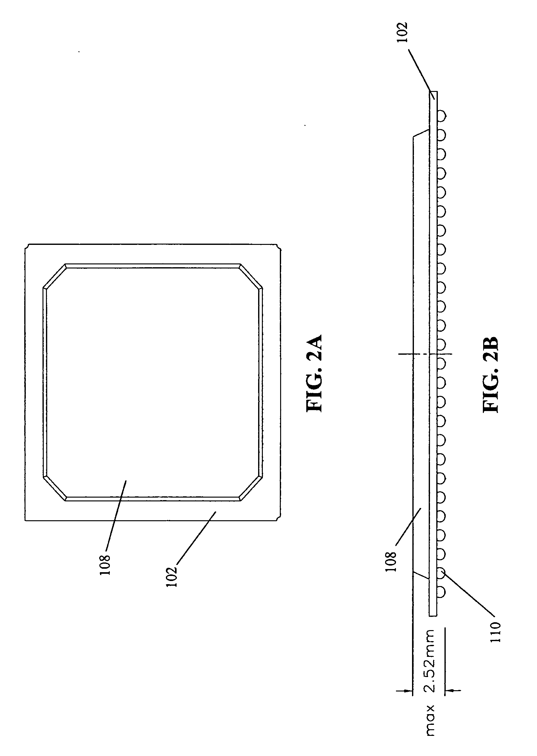
[0081](2) Electrical interconnect pads on the top surface of the encapsulation material allow for fine pitch ball grid array (FBGA) packages shown in FIG. 3 and other chip scale packages that do not have a substantial po...


PUM


Abstract

Apparatuses, methods, and systems for improved integrated circuit packages are described. An integrated circuit (IC) package includes a substrate having opposing first and second surfaces, an IC die, a plurality of conductive elements, and an encapsulating material. The substrate has a plurality of contact pads on the first surface that are electrically coupled to a plurality of electrically conductive features on the second surface. The plurality of conductive elements is formed on the first surface of the substrate. The IC die is located on the first surface of the substrate. The encapsulating material encapsulates the IC die and a portion of each element of the plurality of conductive elements.

Description

[0001]This application claims the benefit of U.S. Prov. Appl. No. 60 / 799,657, filed May 12, 2006, which is incorporated by reference herein in its entirety.BACKGROUND OF THE INVENTION[0002]1. Field of the Invention[0003]The present invention relates to integrated circuit (IC) device packaging technology. More specifically, the invention relates to stacked packages.[0004]2. Related Art[0005]The die-up plastic ball grid array package was first introduced by Motorola and was called Overmolded Plastic Pad Array Carriers (OMPAC). For further detail on this package type, refer to “Overmolded Plastic Pad Array Carriers (OMPAC): A Low Cost, High Interconnect Density IC Packaging Solution for Consumer and Industrial Electronics,” Electronic Components and Technology Conference, IEEE, pp. 176-182, 1991, which is incorporated by reference herein in its entirety. Commonly known as a “PBGA” package, the plastic ball grid array (PBGA) package features a plastic printed circuit board (substrate) t...

Claims


Application Information

Patent Timeline
Patent Type & Authority Applications(United States)
IPC IPC(8): H01L23/28
CPCH01L21/56H01L21/561H01L23/3128H01L23/49816H01L24/97H01L25/105H01L2224/48091H01L2224/48225H01L2224/48228H01L2224/48465H01L2224/73265H01L2224/97H01L2225/06568H01L2924/01013H01L2924/01015H01L2924/01029H01L2924/01033H01L2924/01079H01L2924/01082H01L2924/01327H01L2924/09701H01L2924/14H01L2924/15311H01L2924/1532H01L2924/15331H01L2924/19041H01L2924/19042H01L2924/19043H01L24/48H01L2924/01087H01L2924/014H01L25/50H01L2224/32225H01L2224/48227H01L2224/48237H01L2225/1023H01L2225/1058H01L2924/00014H01L2224/83H01L2224/85H01L2924/00H01L2924/00012H01L2924/15787H01L24/73H01L2924/181H01L2224/48471H01L2224/45099H01L2224/45015H01L2924/207H01L23/12
Inventor KHAN, REZAUR RAHMANZHAO, SAM ZIQUN
Owner AVAGO TECH WIRELESS IP SINGAPORE PTE
Why Eureka
Try Eureka