Electro-optical device and image forming apparatus

a technology of optical devices and image forming apparatus, which is applied in the direction of static indicating devices, multiplex communication, instruments, etc., can solve the problems of reducing affecting so as to improve the resolution of electro-optical elements and reduce the dimensions of drive circuits.

Inactive Publication Date: 2007-11-29
SEIKO EPSON CORP
View PDF5 Cites 19 Cited by
  • Summary
  • Abstract
  • Description
  • Claims
  • Application Information

AI Technical Summary

Benefits of technology

[0007]Embodiments of the invention improve the resolution of electro-optical elements while reducing the dimensions of a drive circuit that drives the electro-optical elements.

Problems solved by technology

In contrast, a reduction in the dimensions of the drive circuit degrades the resolution of the electro-optical elements.
If the size of the terminals (the first terminal and the second terminal) on the substrate is excessively reduced, a connection failure is more likely to occur between the terminals and the output terminals of the electronic component.
This puts a limit to the degree of size reduction of the terminals.

Method used


Image

  • Electro-optical device and image forming apparatus
  • Electro-optical device and image forming apparatus
  • Electro-optical device and image forming apparatus

Examples


first embodiment

A. First Embodiment

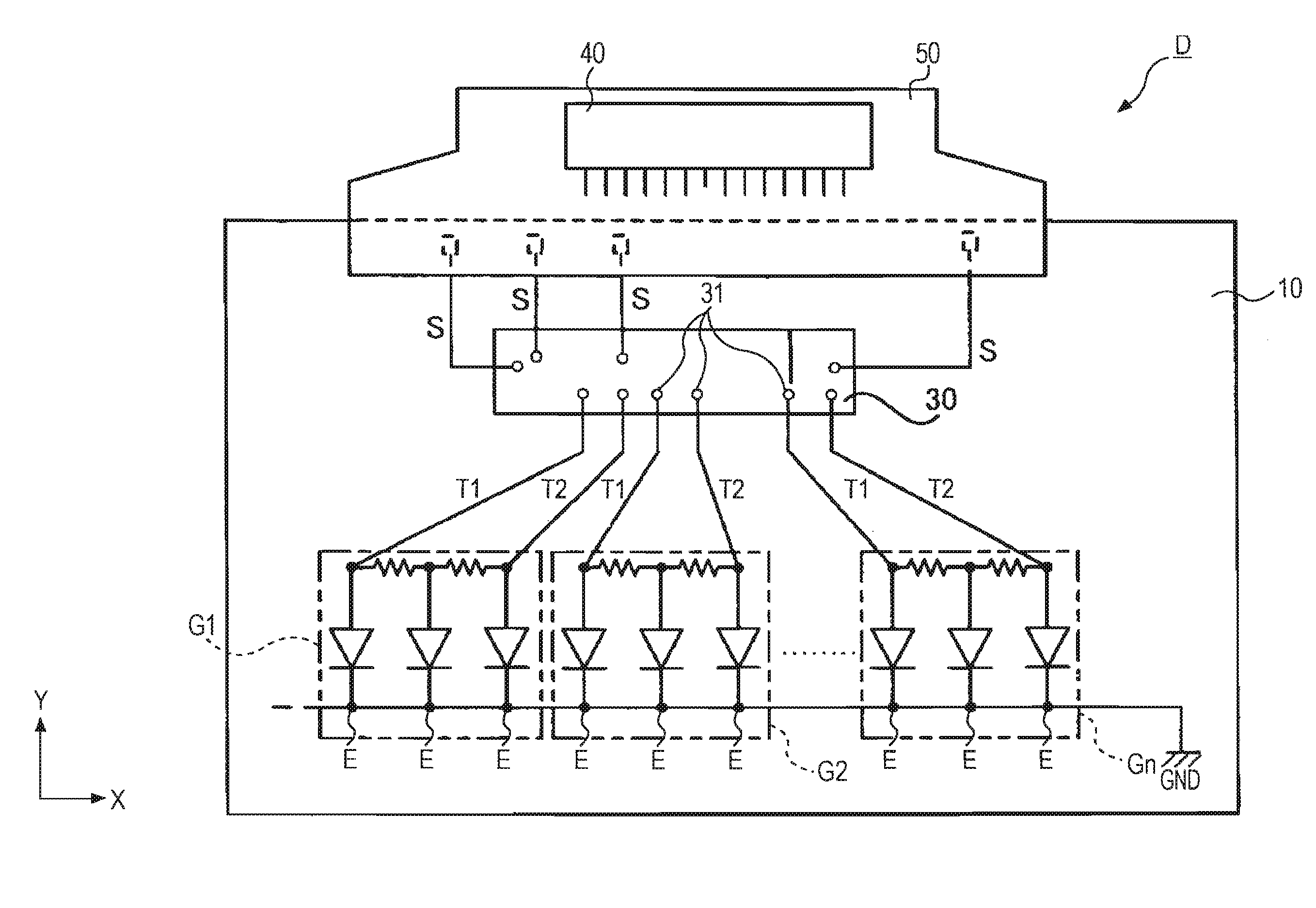
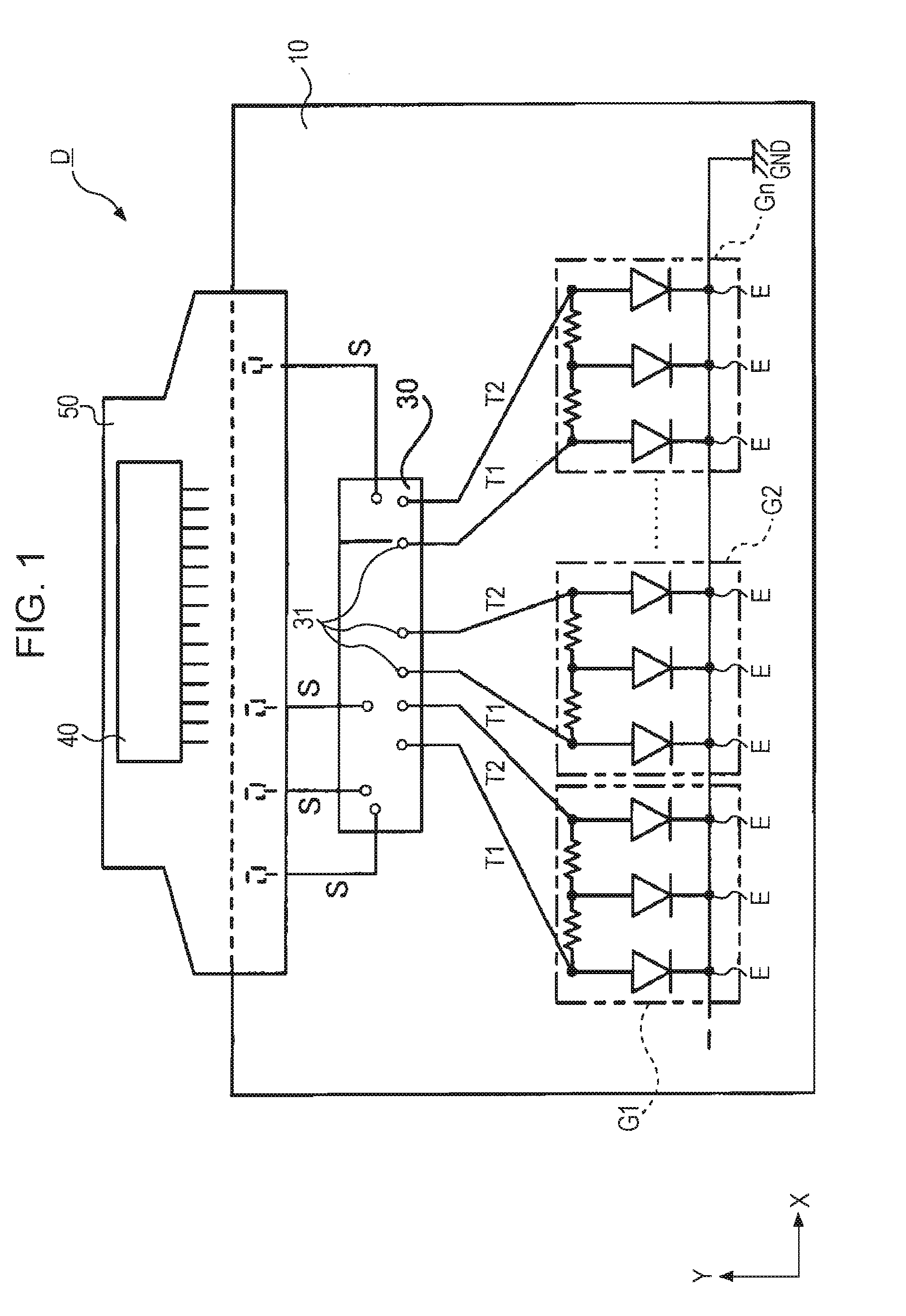
[0032]FIG. 1 is a plan view of an exemplary structure of an electro-optical device D according to a first embodiment of the invention. The electro-optical device D is used, for example, as an exposure device for forming a latent image on a photosensitive member in an electrophotographic image forming apparatus. As shown in FIG. 1, the electro-optical device D has a substrate 10 and a plurality of electro-optical elements E formed on a surface of the substrate 10. The electro-optical elements E are arranged in two lines along the X-direction (main scanning direction) in a zigzag pattern. The electro-optical elements E according to the first embodiment are organic light-emitting diodes, each having a light-emitting layer made of an organic electroluminescent (EL) material and an anode and a cathode sandwiching the light-emitting layer. Each of the electro-optical elements E emits light with brightness according to current supplied to the light-emitting layer. The el...

second embodiment

B. Second Embodiment

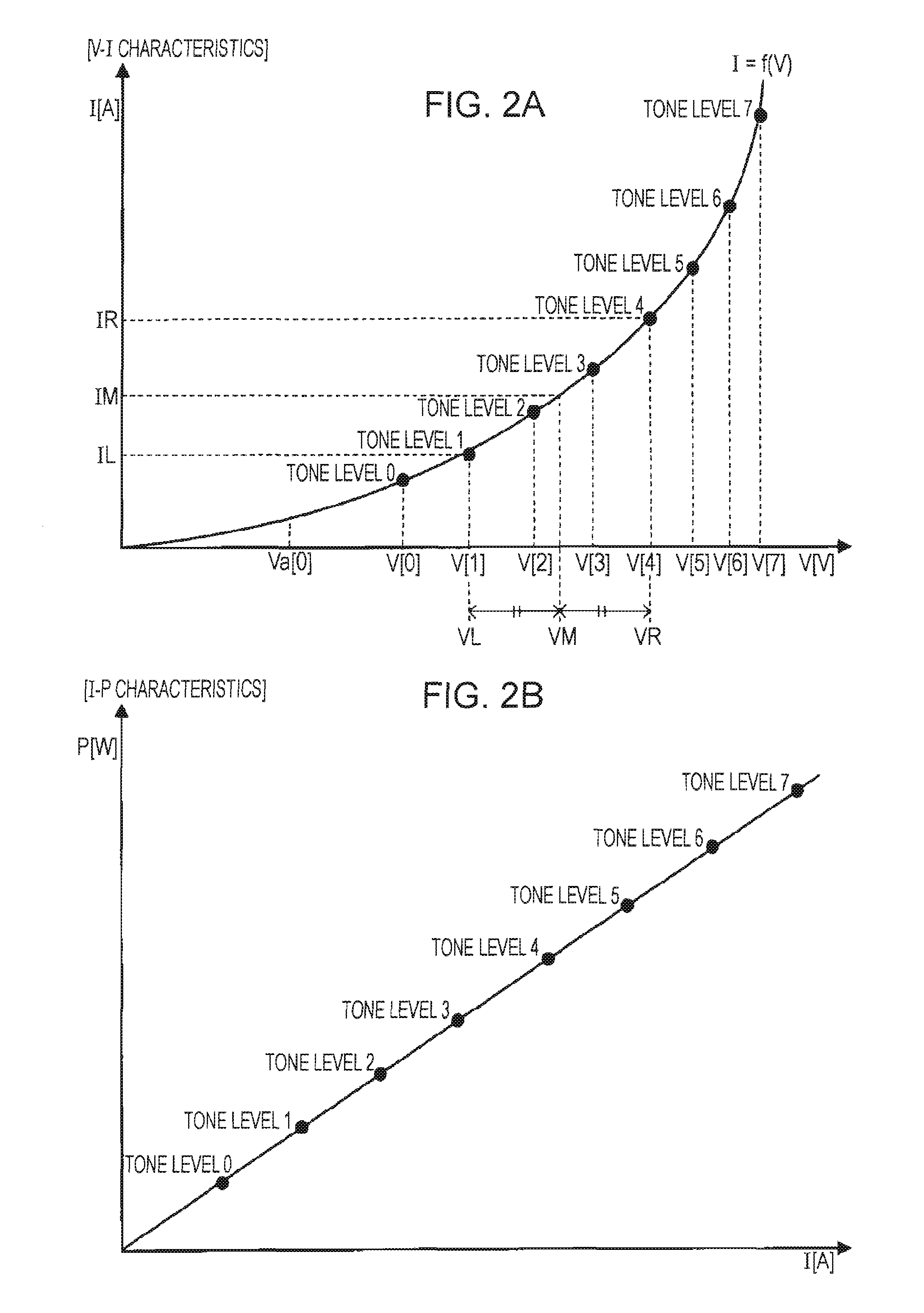
[0054]In the first embodiment, in the case that different tone levels are specified to the electro-optical elements El and ER, the electro-optical element EM provides a tone level between those of the electro-optical elements EL and ER. Since the tone level in a natural image such as a photograph tends to change step by step, the above-described tone-level control scheme (e.g., the on / off states shown in FIG. 5C) is preferable. However, in the case of an image mainly including lines such as sentences and diagrams (hereinafter referred to as a “data image”), it is preferable that the shades of tones be clearly distinguished (e.g., the on / off states shown in FIG. 5D) in contrast to a natural image such as a photograph where the tone level tends to change continuously. According to a second embodiment, in the case that an image to be output (hereinafter referred to as an “output image”) is a data image, the voltage value of each drive voltage is set such that the bo...

third embodiment

C. Third Embodiment

[0058]In the first and second embodiments, the anodes of the electro-optical elements EL, EM, and ER are separated from one another. Alternatively, an anode may be continuous across a point at which the drive voltage VL is applied and a point at which the drive voltage VR is applied.

[0059]Portions (a) to (c) of FIG. 8 illustrate a drive method according to a third embodiment of the invention. Sections corresponding to those in the first embodiment are referred to using the same reference numerals, and descriptions thereof are omitted where appropriate.

[0060]As shown in portion (a) of FIG. 8, the electro-optical device D has an electro-optical layer (light-emitting layer) 200 made of an electro-optical material, such as an organic EL material, a cathode 300 continuous over the entire electro-optical layer 200, and a plurality of anodes 100 facing the cathode 300 with the electro-optical layer 200 provided therebetween. The anodes 100 are separated from one another....


PUM


Abstract

An electro-optical device includes a first electro-optical element, a second electro-optical element, and a third electro-optical element. A first node is electrically connected to the first electro-optical element, a second node is electrically connected to the second electro-optical element, and a third node electrically connected to the third electro-optical element. A first resistor placed between the first node and the third node and a second resistor placed between the second node and the third node. Additionally, a first signal supplying unit that supplies a first signal to the first node and a second signal supplying unit that supplies a second signal to the second node.

Description

CROSS-REFERENCE TO RELATED APPLICATION[0001]This application claims priority from Japanese Patent Application No. 2006-146431 filed in the Japanese Patent Office on May 26, 2006, the entire disclosure of which is hereby incorporated by reference in its entirety.BACKGROUND[0002]1. Technical Field[0003]Embodiments of the present invention include techniques for controlling tone levels of electro-optical elements, such as organic light-emitting diodes or the like.[0004]2. Related Art[0005]Electro-optical devices having an arrangement of electro-optical elements, such as organic light-emitting diodes or the like, are widely used in electronic apparatuses, such as image forming apparatuses and display apparatuses. For example, JP-A-2006-62162 discloses a light-emitting device in which a drive circuit is mounted on a surface of a substrate having an arrangement of many electro-optical elements. The tone level of each electro-optical element is controlled in accordance with a signal suppli...

Claims


Application Information

Patent Timeline
Patent Type & Authority Applications(United States)
IPC IPC(8): G09G3/10H04J14/08
CPCG09G3/14G09G3/2011G09G2330/021G09G2300/0465G09G3/3216H05B33/02H05B33/06
Inventor WAKABAYASHI, JUNICHIOZAWA, TOKURO
Owner SEIKO EPSON CORP
Why Eureka
Try Eureka