Switching Power Supply Apparatus
- Summary
- Abstract
- Description
- Claims
- Application Information
AI Technical Summary
Benefits of technology
Problems solved by technology
Method used
Image
Examples
first embodiment
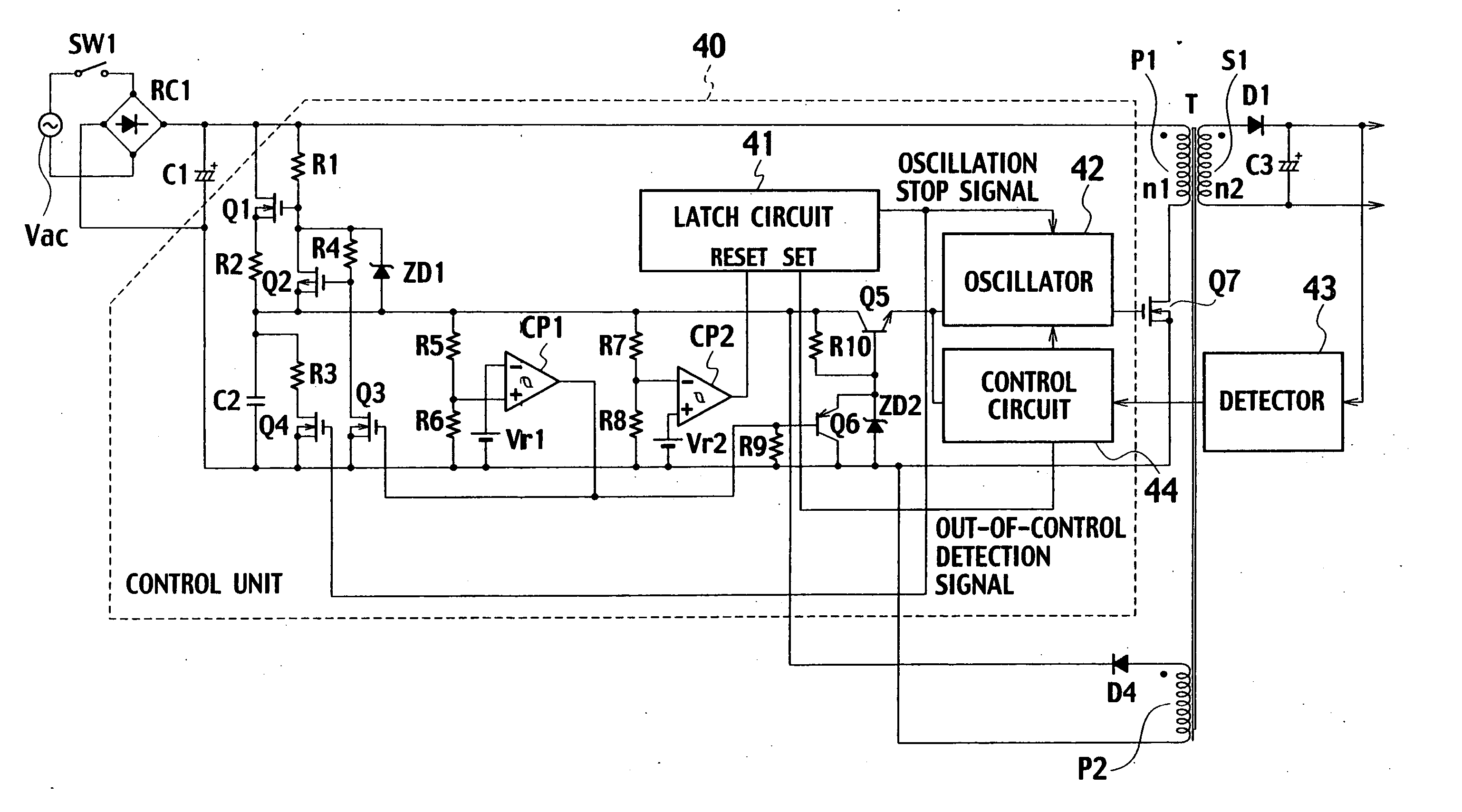
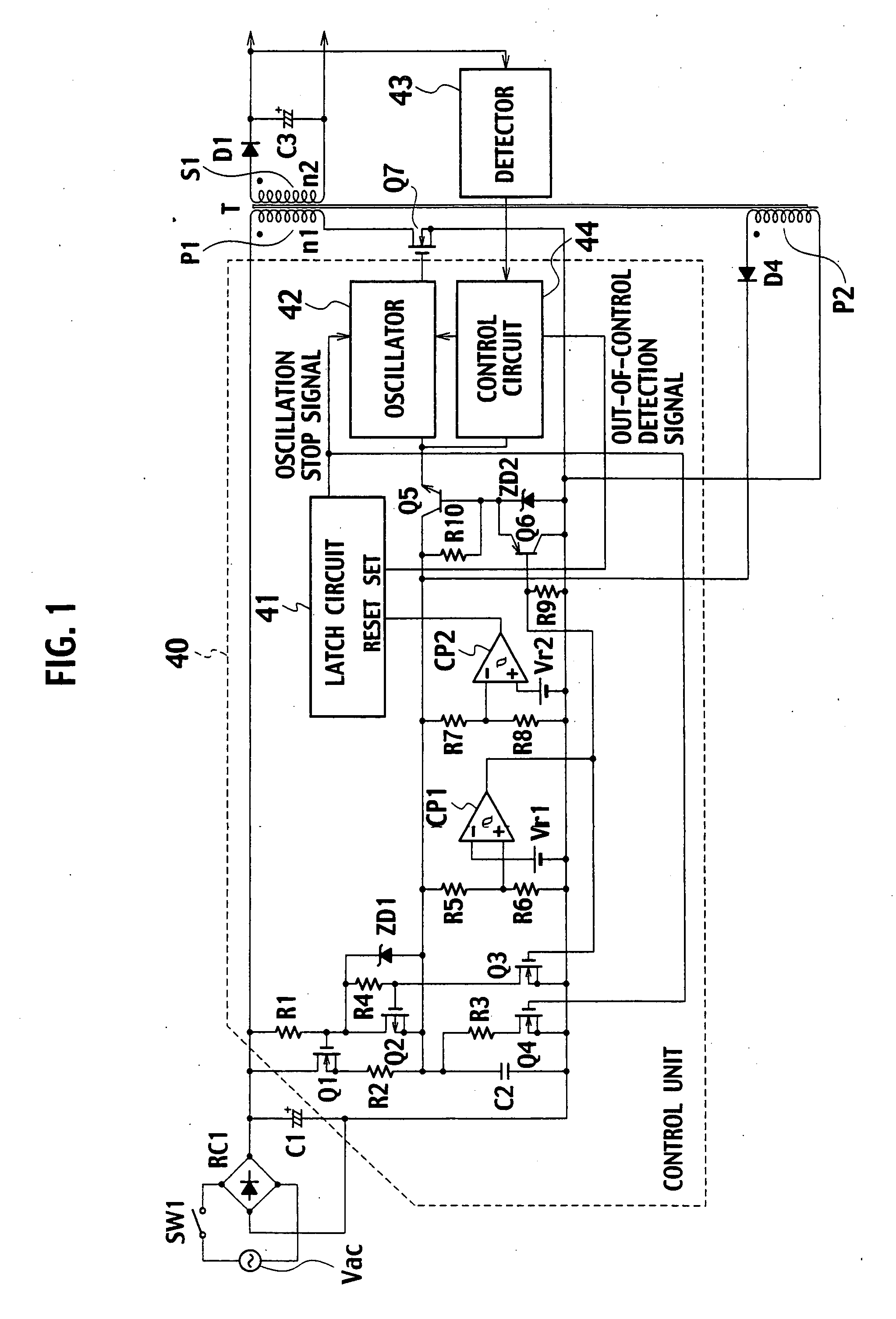
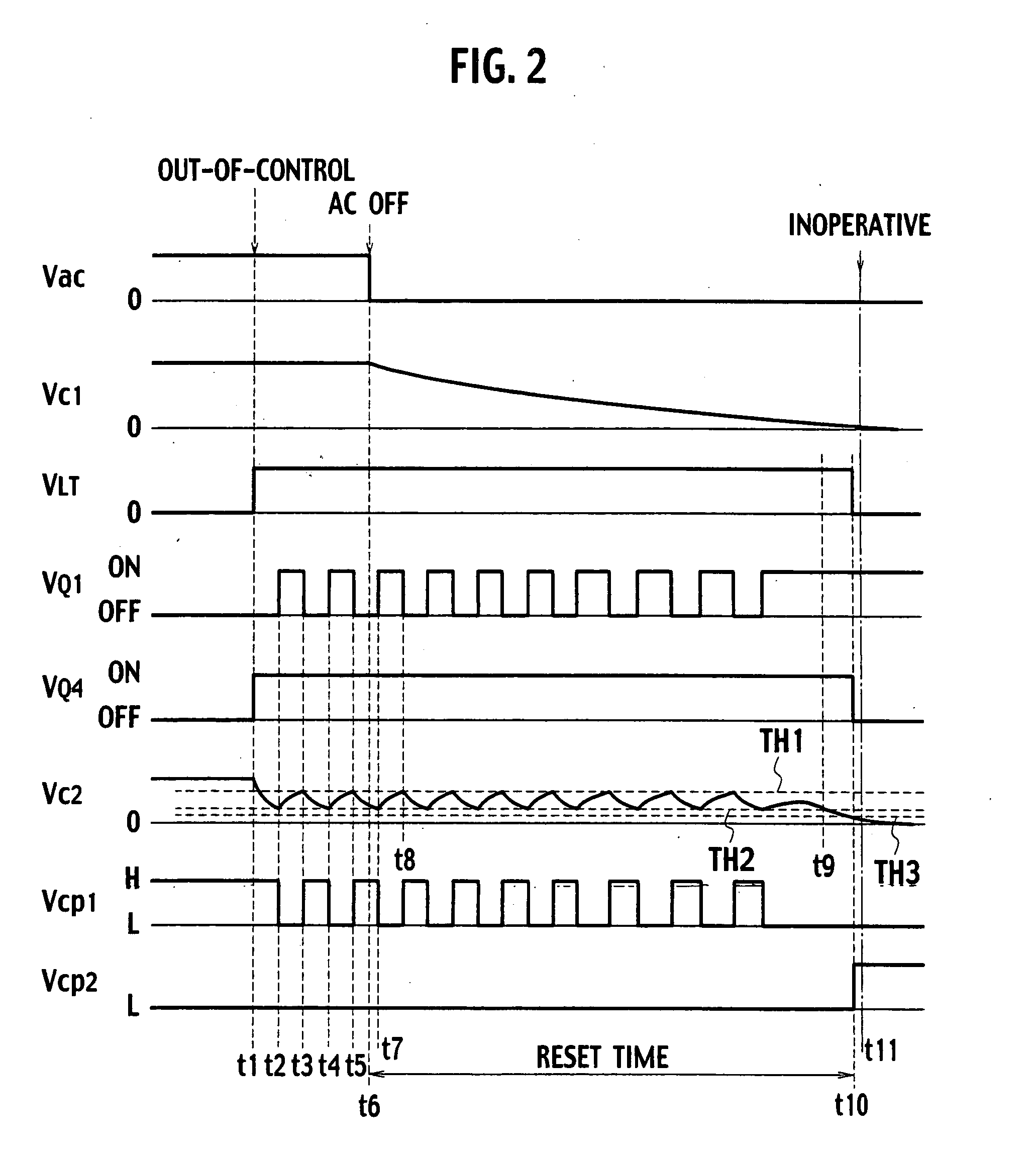
[0039]FIG. 4 is a circuit configuration diagram of a switching power supply apparatus according to a first embodiment of the present invention. In the conventional switching power supply apparatus shown in FIG. 1, for the current passing through the FET Q1, a current is set such that satisfies a function at each time of actuating, stopping, and operating the latch circuit (i.e. the time of output of the oscillation stop signal) and that does not excessively heat the FET Q1. Therefore, for the current of the FET Q1, a large current is not required, and even if the smoothing capacitor C1 is discharged by the actuation circuit when the latch circuit 41 is set to switch off the switch SW1, the reset time cannot be shortened.
[0040] In the switching power supply apparatus according to the first embodiment shown in FIG. 4, in addition to the conventional switching power supply apparatus, an overheat detector 45, an AND circuit 46, an inverter 47, NAND circuits 48, 49, and 50, a comparator...
second embodiment
[0058]FIG. 6 is a circuit configuration diagram of a switching power supply apparatus according to a second embodiment of the present invention. In the second embodiment shown in FIG. 6, by checking an alternating input voltage, when there is no alternating current input, the FET Q1 is kept to be ON state all time, a FET Q9 is turned on, and the FET Q8 is turned on. Thus, a resistor R11 is short-circuited to increase the current passing through the actuation circuit, thereby further efficiently discharging the electrical charge of the smoothing capacitor C1, and shortening the reset time.
[0059] As shown in FIG. 6, an anode of a diode D2 is connected to one end TP1 of a full-wave rectifier circuit RC1, and an anode of a diode D3 is connected to another end TP2 of the full-wave rectifier circuit RC1. Cathodes of the diode D2 and the diode D3 are commonly connected, and this connection point is connected to one terminal of each of the resistor R13 and a capacitor C4. To a series circu...
PUM
 Abstract
Description
Claims
Application Information


