Semiconductor Device

a technology of semiconductor devices and semiconductors, applied in semiconductor devices, semiconductor/solid-state device details, electrical apparatus, etc., can solve problems such as failure of connection with respect to mounting boards, and achieve the effects of poor solder wettability, excellent solder wettability, and sufficient solder wettability

Inactive Publication Date: 2007-12-13
ROHM CO LTD
View PDF10 Cites 5 Cited by
  • Summary
  • Abstract
  • Description
  • Claims
  • Application Information

AI Technical Summary

Benefits of technology

[0023] It is an object of the present invention to provide a semiconductor device which ensures that, when the semiconductor device is bonded to a mounting board, the bonding state of the semiconductor device on the mounting board can be easily checked.
[0049] With this arrangement, the coating film ensures an excellent solder wettability even if the main portion does not have a sufficient solder wettability (even if the main portion is composed of a material susceptible to formation of a surface oxide and has a poorer solder wettability due to the oxide). Thus, the connection reliability of the external connection terminal on the mounting board is improved. The coating film may be composed of, for example, a material less susceptible to oxidation than the main portion.

Problems solved by technology

The solder balls 76, 85 having the voids are liable to cause a connection failure with respect to the mounting board.

Method used


Image

  • Semiconductor Device
  • Semiconductor Device
  • Semiconductor Device

Examples


first embodiment

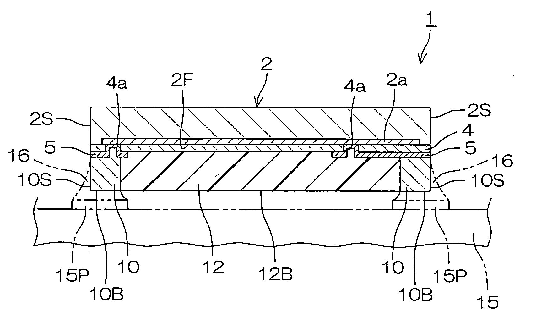
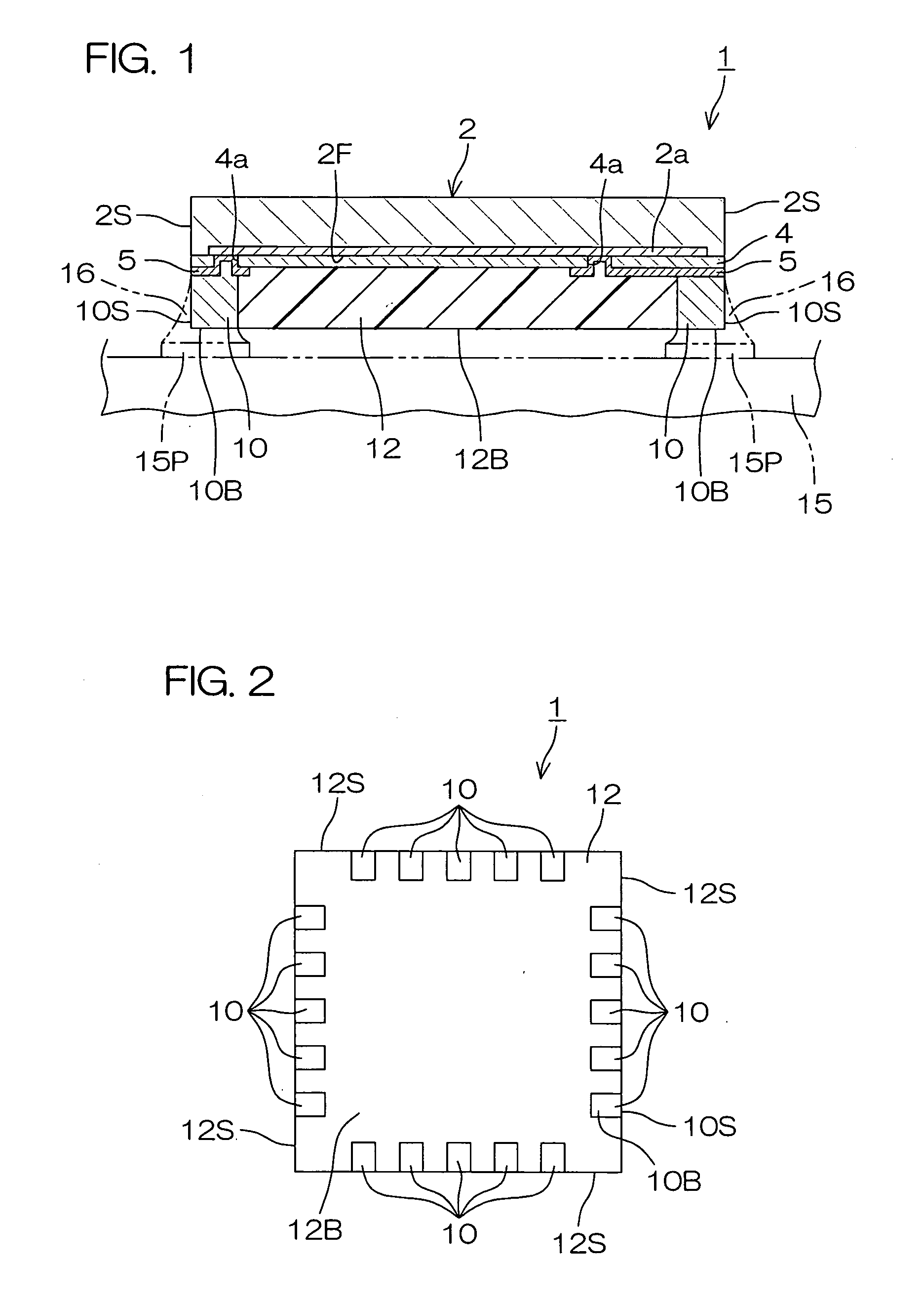
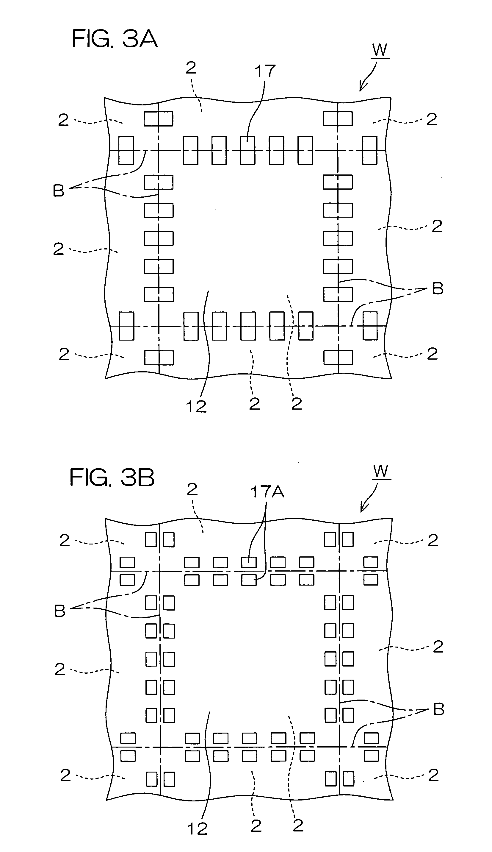
[0067]FIG. 1 is a schematic sectional view illustrating a construction of a semiconductor device according to the present invention, and FIG. 2 is a schematic bottom view of the semiconductor device. The semiconductor device 1 is a so-called chip size package (CSP), and includes a semiconductor chip 2.

[0068] The semiconductor chip 2 includes a semiconductor element 2a provided in one surface (functional surface 2F) thereof. The functional element 2a may be, for example, a transistor. An insulation film 4 is provided on the functional surface 2F as covering the functional element 2a. The insulation film 4 has openings 4a through which electrodes of the functional element 2a are exposed.

[0069] Rewirings 5 respectively electrically connected to the electrodes of the functional element 2a through the openings 4a are provided on the insulation film 4. Further, a protective resin layer 12 is provided over the insulation film 4 as covering the rewirings 5. Side surfaces 2S of the semicond...

second embodiment

[0092]FIG. 4 is a schematic sectional view of a semiconductor device according to the present invention, and FIG. 5 is a schematic bottom view of the semiconductor device. In FIGS. 4 and 5, components corresponding to those shown in FIGS. 1 and 2 will be denoted by the same reference characters as in FIGS. 1 and 2.

[0093] The semiconductor device 21 includes a heat-sink terminal 22 provided in a center portion of the semiconductor chip 2 as seen in plan perpendicularly to the bottom surface 12B. The heat-sink terminal 22 projects from a rewiring 5A provided on the insulation film 4. The insulation film 4 has openings 4b through which electrodes of the functional element 2a are exposed. The rewiring 5A is electrically connected to the electrodes of the functional element 2a through the openings 4b. Therefore, the heat-sink terminal 22 is electrically connected to the functional element 2a.

[0094] The heat-sink terminal 22 extends thickness wise through the protective resin layer 12, a...

third embodiment

[0100]FIG. 6 is a schematic sectional view illustrating a construction of a semiconductor device according to the present invention. In FIG. 6, components corresponding to those shown in FIGS. 1 and 2 will be denoted by the same reference characters as in FIGS. 1 and 2. The semiconductor device 31 is a multi-chip module including a first semiconductor chip 32 and a second semiconductor chip 33.

[0101] The first semiconductor chip 32 includes a first functional element 32a formed in one surface (first functional surface 32F) thereof. An insulation film 4 is provided over the first functional surface 32F as covering the functional element 32a. The insulation film 4 has openings 4a, 4c through which electrodes of the functional element 32a are exposed. Rewirings 5B respectively electrically connected to the electrodes of the functional elements 32a through the openings 4c are provided on the insulation film 4.

[0102] The second semiconductor chip 33 includes a second functional element ...


PUM


Abstract

A semiconductor device (1, 1A, 21, 31, 41, 51) provided with a first semiconductor chip (3) having a first functional surface (3F) formed with a first functional element (3a), a protective resin layer (12) provided on the first functional surface, and an external connection terminal (10, 19, 52) provided on a peripheral portion of the first functional surface for external electrical connection, the external connection terminal having a bottom surface (10B, 19BB) exposed from a bottom surface (12B) of the protective resin layer facing away from the first functional surface and a side surface (10S, 19BS) exposed from a side surface (12S) of the protective resin layer.

Description

TECHNICAL FIELD [0001] The present invention relates to a semiconductor device having substantially the same size as a semiconductor chip. BACKGROUND ART [0002] In recent years, semiconductor devices have been required to have a smaller size and a higher mounting density. The semiconductor devices satisfying such requirements include a chip size package (CSP; disclosed in the following Patent Publication 1) and a multi-chip module (MCM; disclosed in the following Patent Publication 2). [0003]FIG. 12 is a schematic sectional view illustrating a construction of a prior art semiconductor device having a chip size package structure. [0004] The semiconductor device 71 includes a semiconductor chip 72. The semiconductor chip 72 includes a functional element 72a formed in one surface thereof, and an insulation film 73 covering the functional element 72a. The insulation film 73 has openings 73a through which electrodes of the functional element 72a are exposed. [0005] Rewirings 74 arranged ...

Claims


Application Information

Patent Timeline
Patent Type & Authority Applications(United States)
IPC IPC(8): H01L23/12
CPCH01L23/3114H01L24/10H01L24/13H01L2924/014H01L2924/01006H01L2924/01005H01L24/48H01L2924/19043H01L2924/15311H01L2924/01079H01L2924/01078H01L2924/01075H01L2924/01074H01L2924/01033H01L2924/01029H01L2924/01004H01L25/0657H01L2224/13099H01L2224/32145H01L2224/32225H01L2224/48091H01L2224/48227H01L2224/73265H01L2225/06513H01L2225/06527H01L2225/06551H01L2225/06582H01L2924/00014H01L2924/00H01L2924/181H01L2224/13H01L2224/05548H01L2224/05573H01L2224/02377H01L2224/05599H01L2924/00012H01L2224/45099H01L2224/45015H01L2924/207H01L23/12
Inventor TANIDA, KAZUMASAHIGUCHI, SHIGOKADOGUCHI, TAKUYA
Owner ROHM CO LTD
Why Eureka
Try Eureka