Semiconductor device having a resistance for equalizing the current distribution

a technology of current distribution and resistance, which is applied in the direction of semiconductor devices, semiconductor/solid-state device details, electrical apparatus, etc., can solve the problems of resistance value elevated and gradual cracking of the solder, and achieve the effect of preventing open-circuit defect of gate balance resistance and ensuring high reliability

Inactive Publication Date: 2007-12-13
MITSUBISHI ELECTRIC CORP
View PDF9 Cites 0 Cited by
  • Summary
  • Abstract
  • Description
  • Claims
  • Application Information

AI Technical Summary

Benefits of technology

[0007]The present invention has been developed to solve the above-described problems, and therefore it is an object of the present invention to provide a semiconductor device that can prevent open-circuit defect of the gate balance resistance generated in the operation of the semiconductor device and can secure high reliability.

Problems solved by technology

Consequently, in the soldered portion, thermal stress caused by difference of coefficients of linear thermal expansion of each constituting member is generated, and the solder is gradually cracked.
When the portion where the gate balance resistance is soldered is cracked, there has been a problem wherein the resistance value is elevated, and finally open-circuit defect is caused to generate withstand voltage defect.

Method used


Image

  • Semiconductor device having a resistance for equalizing the current distribution
  • Semiconductor device having a resistance for equalizing the current distribution
  • Semiconductor device having a resistance for equalizing the current distribution

Examples


first embodiment

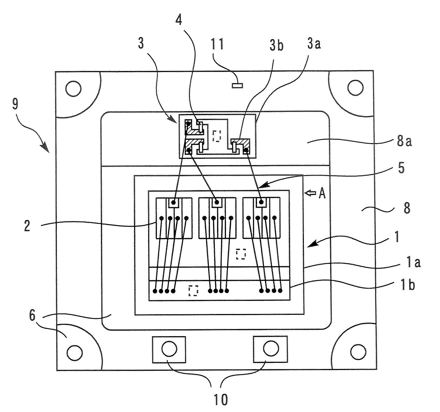
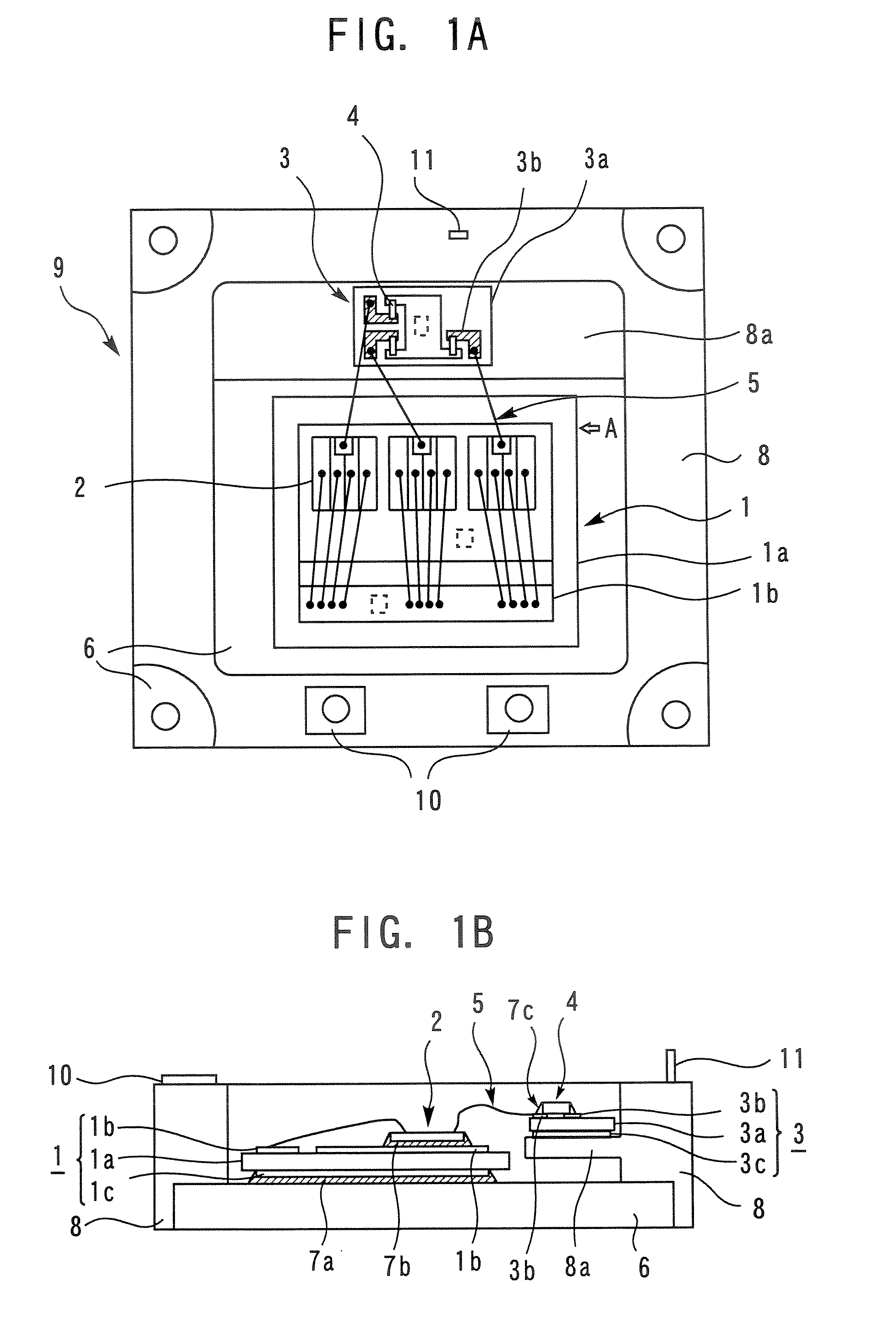
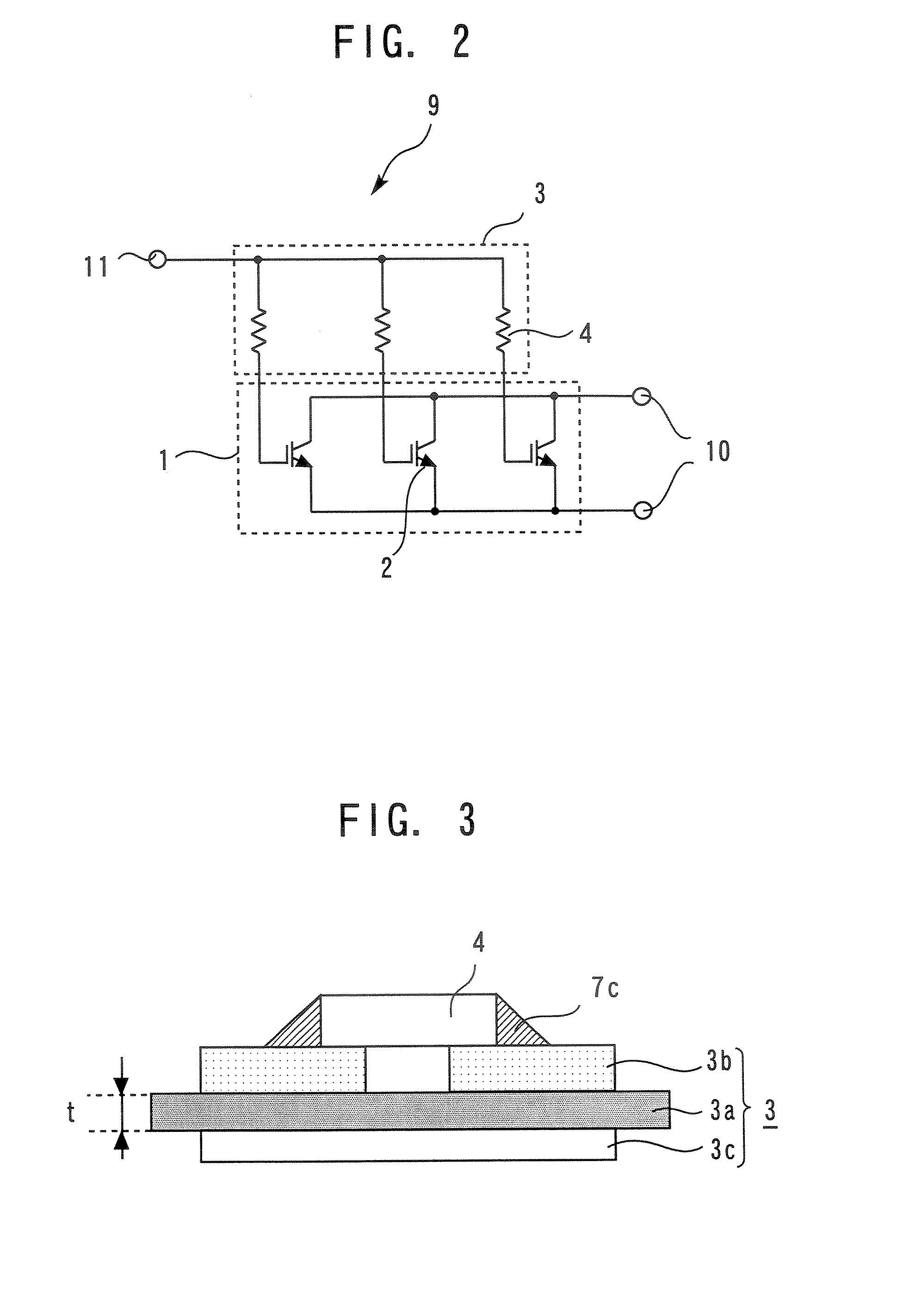
[0020]A semiconductor device according to the first embodiment will be described. FIG. 1A is a plane view of the semiconductor device according to the present invention; and FIG. 1B is a side view of the semiconductor device viewed from the A direction in FIG. 1A. The semiconductor device is equipped with a heat sink 6 composed of a metal, such as copper and aluminum, and a first insulating substrate 1 is formed on the heat sink 6. The first insulating substrate 1 has a first insulating layer 1a, a first conductive pattern 1b, and a first back face pattern 1c. The first conductive pattern 1b is formed on the upper surface of the first insulating layer 1a, and the first back face pattern 1c is formed on the lower surface of the first insulating layer 1a. The first insulating layer 1a is composed of a ceramic, such as AlN (aluminum nitride), and the first conductive pattern 1b and the first back face pattern 1c, which are joined to the first insulating layer 1a, are formed of copper o...

second embodiment

[0032]A semiconductor device according to the second embodiment will be described. Here, the description will be focused around aspects different from the first embodiment.

[0033]In a conventional art, a semiconductor element 2 and a resistance element 4 were formed on the same insulating substrate. Consequently, the insulating substrate required an insulation resistance to several thousands of volts. However in the first embodiment, an insulating substrate on which a gate balance resistance had been mounted was fixed on the side of the insulating resin casing. Therefore, it is considered to be sufficient if the insulating substrate has an insulation resistance to several tens of volts. For this reason, the second embodiment has a structure wherein the thickness of the insulating layer in the insulating substrate on which a gate balance resistance is mounted is thinner than the thickness of the insulating layer in the insulating substrate on which a semiconductor device is mounted.

[0...

third embodiment

[0038]A semiconductor device according to the third embodiment will be described. Here, the description will be focused around aspects different from the first and second embodiments.

[0039]The plane views of the first insulating substrate 1 and the second insulating substrate 3 of a semiconductor device according to the third embodiment are shown in FIGS. 4A and 4B, respectively. In FIG. 4A, the shortest distance from the periphery of the first conductive pattern 1b to the periphery of the first insulating layer 1a along the surface of the first insulating layer 1a, namely the creeping distance from the first conductive pattern 1b to the periphery of the first insulating layer 1a is represented by D1. In FIG. 4B, the shortest distance from the periphery of the second conductive pattern 3b to the periphery of the second insulating layer 3a along the surface of the second insulating layer 3a, namely the creeping distance from the second conductive pattern 3b to the periphery of the se...


PUM


Abstract

A first insulating substrate is formed on a heat sink, and a semiconductor element is formed thereon. An insulating resin casing is formed so as to cover the first insulating substrate and the semiconductor element. A second insulating substrate is mounted inside the insulating resin casing apart from the first insulating substrate. On the second insulating substrate, a resistance element that functions as a gate balance resistance is fixed by soldering. The second insulating substrate on which the resistance element was thus mounted was made apart from the first insulating substrate on which the semiconductor element was mounted, and was mounted on the side of the insulating resin casing.

Description

BACKGROUND OF THE INVENTION[0001]1. Field of the Invention[0002]The present invention relates to a semiconductor device, and specifically to a semiconductor device on which a resistance is mounted to even out the current distribution to semiconductor elements of the semiconductor device.[0003]2. Background Art[0004]In a semiconductor device used in the inverter / converter of electric railways or the like, a rated current of several-hundred to several-thousand amperes is required. Therefore, several to several-ten semiconductor elements are normally connected in parallel in a semiconductor device.[0005]For example, in Japanese Unexamined Patent Publication No. 2001-185679, the above-described semiconductor device, which has a plurality of semiconductor elements formed on an insulating substrate, is disclosed. On the insulating substrate, a resistance known as a gate balance resistance is disposed in the vicinity of each semiconductor element. The resistance is to even out the current ...

Claims


Application Information

Patent Timeline
Patent Type & Authority Applications(United States)
IPC IPC(8): H01L23/48
CPCH01L23/647H01L25/162H01L25/165H01L2224/48091H01L2924/13055H01L2224/73265H01L2224/48137H01L2924/13091H01L2224/49111H01L2924/00014H01L2924/00
Inventor KOGA, MASUOMIZOSHIRI, TETSUOHAYASHIDA, YUKIMASA
Owner MITSUBISHI ELECTRIC CORP
Why Eureka
Try Eureka