Methods and apparatus for simulating distributed effects

a distributed effect and simulation method technology, applied in the field can solve the problems of complex modeling of large-area semiconductor devices, non-uniform current flow, and non-uniform behavior across devices

Inactive Publication Date: 2007-12-13
NXP USA INC
View PDF4 Cites 123 Cited by
  • Summary
  • Abstract
  • Description
  • Claims
  • Application Information

AI Technical Summary

Problems solved by technology

The modeling of large-area semiconductor devices is complicated by the presence of distributed effects—i.e., parasitic capacitances, inductances, and resistances that are inherent in the device and interconnect structure.
Such parasitics typically lead to non-uniform current flow and non-uniform behavior across the device, and can therefore significantly degrade the assumed scaling relationships while having a substantial impact on real-world performance of the design.
These elements and their interconnection, which reflect the layout of the device, are distilled into a suitable “netlist.” However, generation of this netlist from the layout, in a standard analog design flow, is not straightforward.
Furthermore, known methods of generating this netlist typically overestimate and / or underestimate the effects of various physical features.

Method used


Image

  • Methods and apparatus for simulating distributed effects
  • Methods and apparatus for simulating distributed effects
  • Methods and apparatus for simulating distributed effects

Examples


Embodiment Construction

[0014]The following detailed description is merely exemplary in nature and is not intended to limit the invention or the application and uses of the invention. Furthermore, there is no intention to be bound by any expressed or implied theory presented in the preceding technical field, background, or the following detailed description. Conventional terms and processes relating to semiconductor manufacturing, component modeling, device layout, and simulation techniques are known to those skilled in the art, and are therefore not discussed in detail herein.

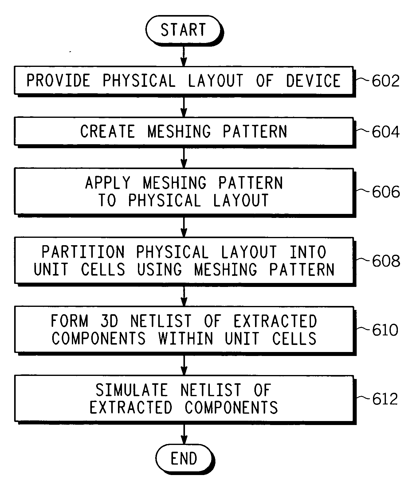
[0015]In general, various embodiments of the present invention relate to systems and methods for simulating distributed effects by providing a meshing pattern (e.g., a two-dimensional meshing pattern that is part of a recognition layer), applying that meshing pattern to the physical layout, and partitioning the physical layout into a three-dimensional netlist of components derived from the unit cells, thereby modeling the parasitics ...


PUM


Abstract

In general, various embodiments of the present invention relate to systems and methods for simulating distributed effects by providing a meshing pattern (200) (e.g., a two-dimensional meshing pattern that is part of a recognition layer), applying that meshing pattern to the physical layout (100), and partitioning the physical layout into a three-dimensional netlist (300) of components derived from the unit cells defined by the meshing pattern (200), thereby modeling the parasitics within the design.

Description

CROSS REFERENCE TO RELATED APPLICATIONS.[0001]This application claims priority to International Application Serial Number PCT / RU / 2006 / 000304 filed Jun. 13, 2006.FIELD OF THE INVENTION[0002]The present invention generally relates to large-area semiconductor devices and, more particularly, to methods for simulating parasitic effects in large-area devices.BACKGROUND OF THE INVENTION[0003]The modeling of large-area semiconductor devices is complicated by the presence of distributed effects—i.e., parasitic capacitances, inductances, and resistances that are inherent in the device and interconnect structure. Such parasitics typically lead to non-uniform current flow and non-uniform behavior across the device, and can therefore significantly degrade the assumed scaling relationships while having a substantial impact on real-world performance of the design. In power metal-oxide semiconductor field effect transistors (MOSFETs), for example, the distributed parasitic resistances associated wi...

Claims


Application Information

Patent Timeline
Patent Type & Authority Applications(United States)
IPC IPC(8): G06F17/50G06F30/367G06F30/392
CPCG06F17/5072G06F17/5036G06F30/367G06F30/392
Inventor KNIFFIN, MARGARET L.SHIPITSIN, DMITRY S.ZUNINO, MICHAEL J.
Owner NXP USA INC
Why Eureka
Try Eureka