
Photoelectric conversion layer stack type color solid-state imaging device

a technology of color solid-state imaging and conversion layer, which is applied in the direction of picture signal generators, television system scanning details, television systems, etc., can solve the problems of difficult to read color signals of all the pixels in 1/30 second, imaging device substantially only performs low-sensitivity imaging, and image quality of moving image of dark scene becomes very low, so as to achieve high sensitivity and large s/n

Active Publication Date: 2007-12-20
FUJIFILM CORP
View PDF3 Cites 26 Cited by
  • Summary
  • Abstract
  • Description
  • Claims
  • Application Information

AI Technical Summary

Benefits of technology

[0018]An object of the present invention is to provide a hybrid photoelectric conversion layer stack type color solid-state imaging device capable of producing an image having high image quality even in shooting of a dark scene.
[0038]The invention makes it possible to produce image signals having a large S / N ratio with high sensitivity because image signals can be output through signal addition (pixel addition) in shooting in which the use of flash light is prohibited, in taking of a moving image, or in a like situation.

Problems solved by technology

However, in imaging devices having more than two million pixels, it is difficult to read color signals of all the pixels in 1 / 30 second.
This means a problem that the imaging device substantially performs only low-sensitivity imaging though being capable of high-sensitivity imaging.
However, since flash light cannot be used in taking a moving image, the image quality of a moving image of a dark scene becomes very low.

Method used


Image

  • Photoelectric conversion layer stack type color solid-state imaging device
  • Photoelectric conversion layer stack type color solid-state imaging device
  • Photoelectric conversion layer stack type color solid-state imaging device

Examples


embodiment 1

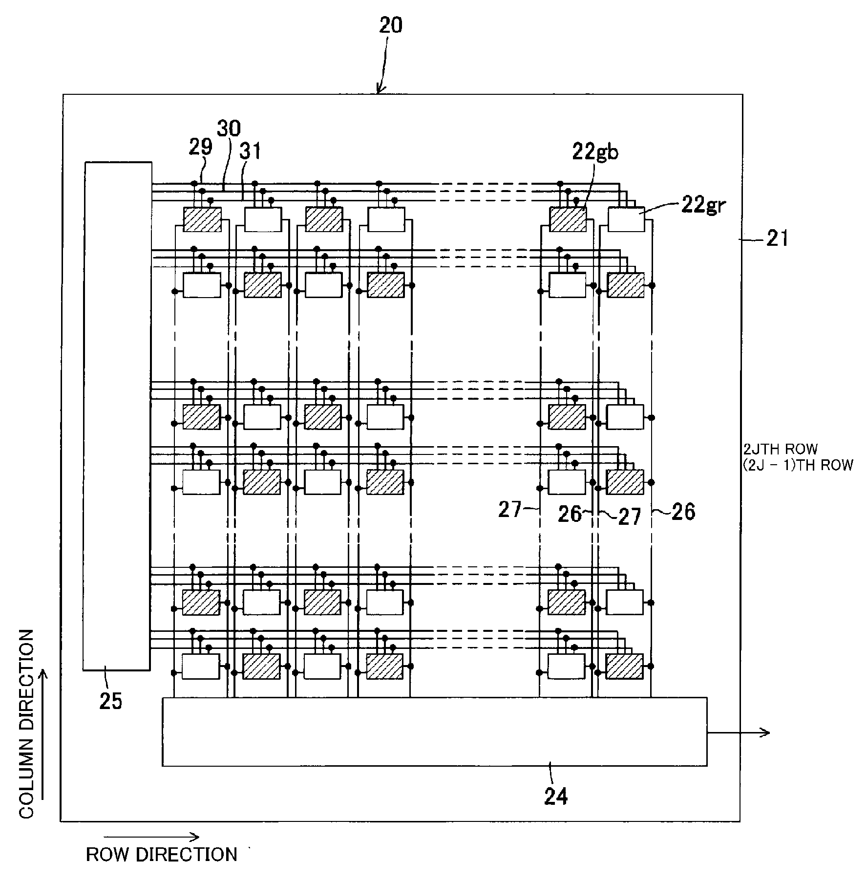
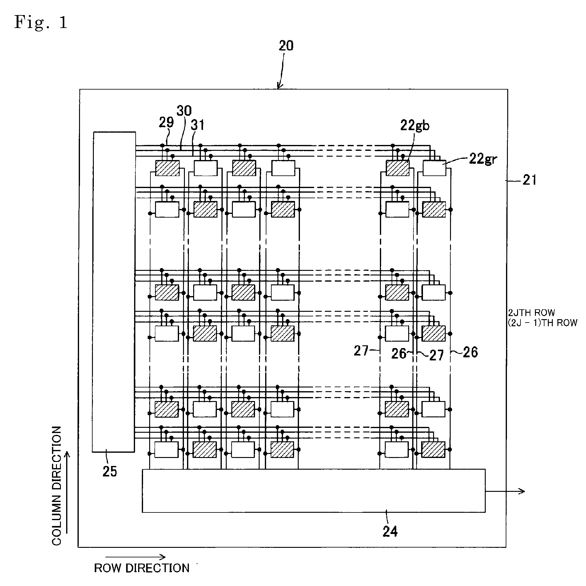
[0082]FIG. 1 schematically shows the surface of a hybrid photoelectric conversion layer stack type color solid-state imaging device according to a first embodiment of the invention. In the photoelectric conversion layer stack type color solid-state imaging device 20, plural, two-kinds of unit pixels 22gb and 22gr are arranged in square lattice form on a semiconductor substrate 21. The unit pixels 22gb which are sensitive to green (G) light and blue (B) light and the unit pixels 22gr which are sensitive to green (G) light and red (R) light are arranged in checkered form (square lattice form).

[0083]An output signal processing section 24 including a row-direction scanning control section is disposed adjacent to the bottom sideline of the semiconductor substrate 21, and a column-direction scanning control section 25 is disposed adjacent to the left sideline of the semiconductor substrate 21. Each unit pixels 22 (in the following, the term “unit pixel 22” is used in referring to both of ...

embodiment 2

[0139]FIG. 6 shows the configuration of an important part of an output signal processing section used in a photoelectric conversion layer stack type color solid-state imaging device according to a second embodiment of the invention. In each correlation double sampling circuit of the output signal processing section of this embodiment, a clamp control switch circuit 67 for making effective or breaking a bypass route of a clamp circuit 57 is provided in the bypass route. The other part of the configuration is the same as in the first embodiment shown in FIGS. 1-5.

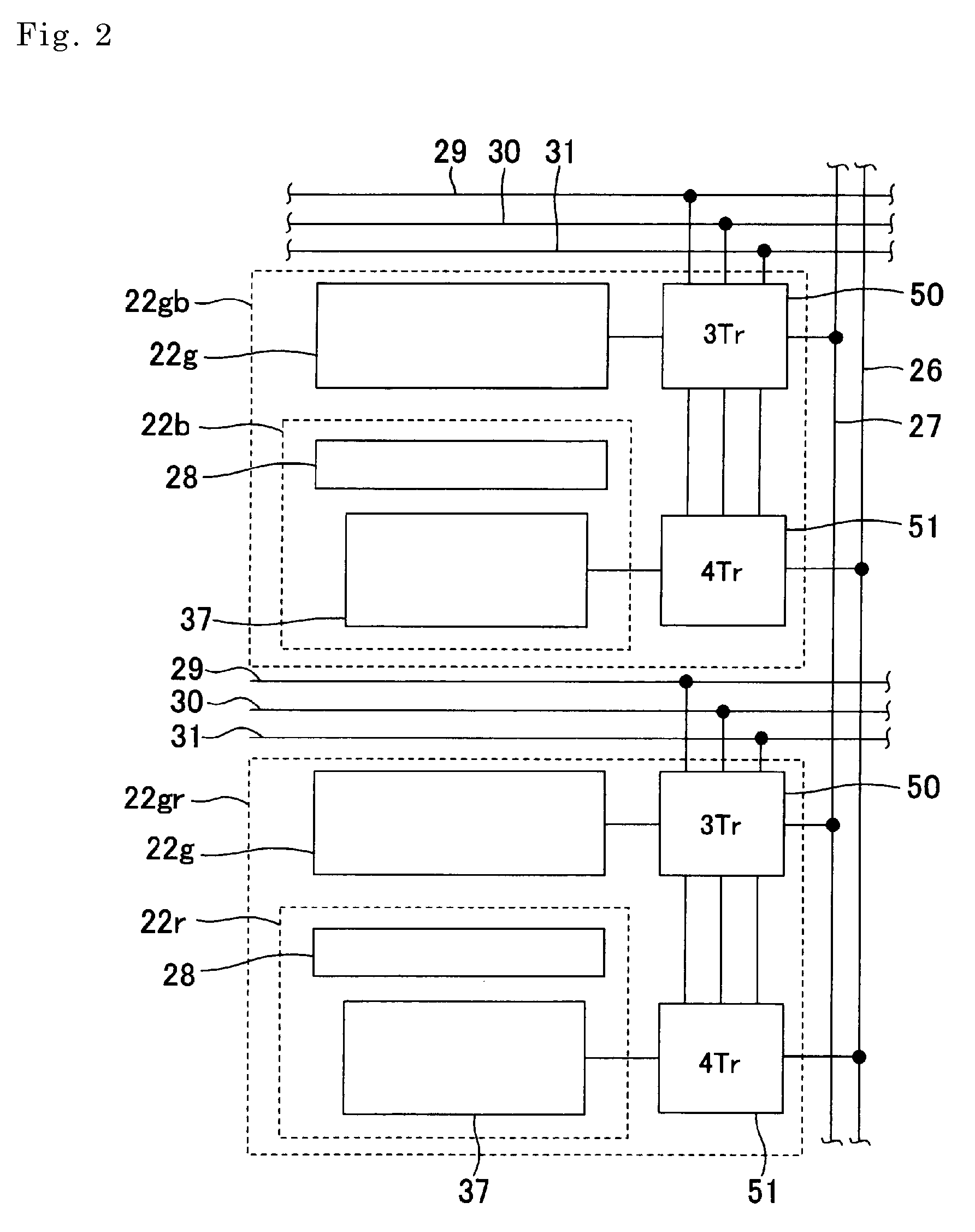
[0140]The first embodiment and this embodiment employ the signal reading circuit 50 having the 3-transistor structure as a signal reading circuit for reading signal charge of each G pixel. Whereas this is intended to lower the degree of an afterimage, the 3-transistor signal reading circuit 50 has a problem that random noise that is superimposed on an output signal of the signal reading circuit 50 cannot be canceled out unlik...

embodiment 3

[0171]FIG. 7 shows the configuration of an important part of an output signal processing section of a photoelectric conversion layer stack type color solid-state imaging device according to a third embodiment of the invention. Whereas in the first and second embodiments the SH selection switch circuits 60 are provided independently of the sample-and-hold circuits 58 and 59, in this embodiment sampling transistors 58a and 59a of the sample-and-hold circuits 58 and 59 also serve as SN selection switches (see FIG. 7).

[0172]An output signal of each clamp circuit 57 is supplied to both sample-and-hold circuits 58 and 59. The sample-and-hold circuit 58 performs a sample-and-hold operation if a sampling pulse is applied to the gate of the sampling transistor 58a, and the sample-and-hold circuit 59 performs a sample-and-hold operation if a sampling pulse is applied to the gate of the sampling transistor 59a. In this manner, the control using a sampling pulse makes it possible to select one ...


PUM


Abstract

A color solid state imaging device as defined herein, which includes an output signal processing section including: signal memory means provided for respective columns of the unit pixels, for holding signals read-cut from the pixels of the same color of the same unit pixel row, respectively; and row-direction scanning control means for switching between an all pixels reading operation in which the signals held by the respective signal memory means are read out individually and output to the outside and a sum reading operation in which among the signals held by the respective signal memory means signals held by signal memory means corresponding to adjoining unit pixels are read out simultaneously and output to the outside.

Description

FIELD OF THE INVENTION[0001]The present invention relates to a photoelectric conversion layer stack type color solid state imaging device in which incident light of one of the three primary colors is detected by a photoelectric conversion layer laid above a semiconductor substrate and incident light of the other two colors that has passed through the photoelectric conversion layer is separated into respective spectral components with color filters and detected by photoelectric conversion elements (photodiodes) formed in the semiconductor substrate. In particular, the invention relates to a photoelectric conversion layer stack type color solid-state imaging device capable of taking color images having high image quality even in shooting of dark scenes.BACKGROUND OF THE INVENTION[0002]In single-plate color solid-state imaging devices as typified by CMOS image sensors, three or four kinds of color filters are arranged in mosaic form on a large number of photoelectric conversion pixels ...

Claims


Application Information

Patent Timeline
Patent Type & Authority Applications(United States)
IPC IPC(8): H04N9/04H04N23/12
CPCH01L27/14621H01L27/14634H01L27/14647H01L27/307H04N9/045H04N2209/047H01L27/302H04N5/335H04N25/00H04N25/134H10K30/57H10K39/32
Inventor SUZUKI, NOBUO
Owner FUJIFILM CORP
Learn More