Micromachine and method of fabricating the same
a micromachine and manufacturing method technology, applied in the field of micromachines, can solve the problems of general deformation of s/n ratio, failure to provide the characteristic quality factor in the ghz band, etc., and achieve the effects of reducing noise component, reducing capacitance, and reducing nois
- Summary
- Abstract
- Description
- Claims
- Application Information
AI Technical Summary
Benefits of technology
Problems solved by technology
Method used
Image
Examples
first embodiment
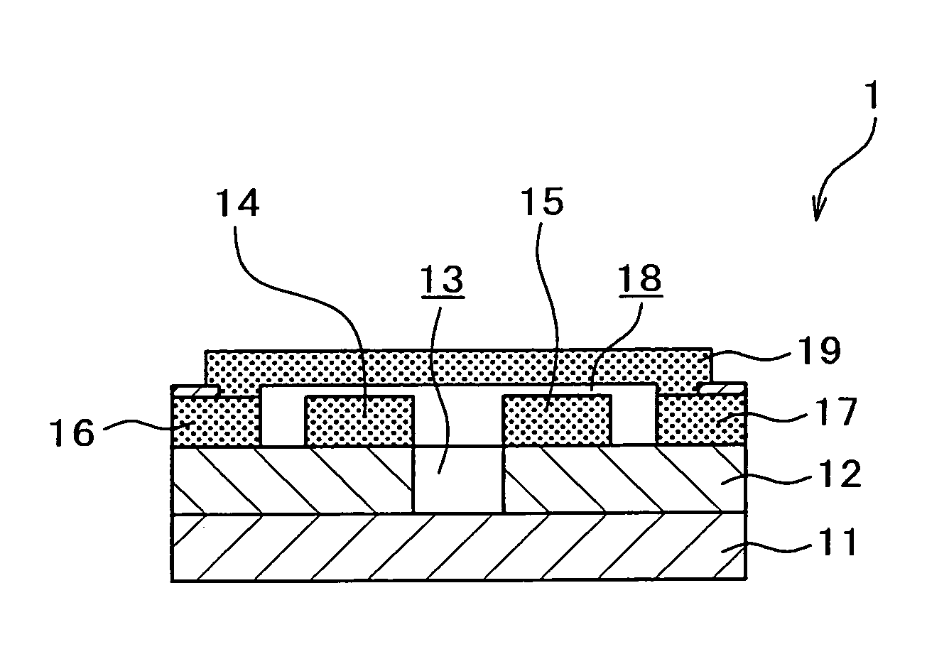
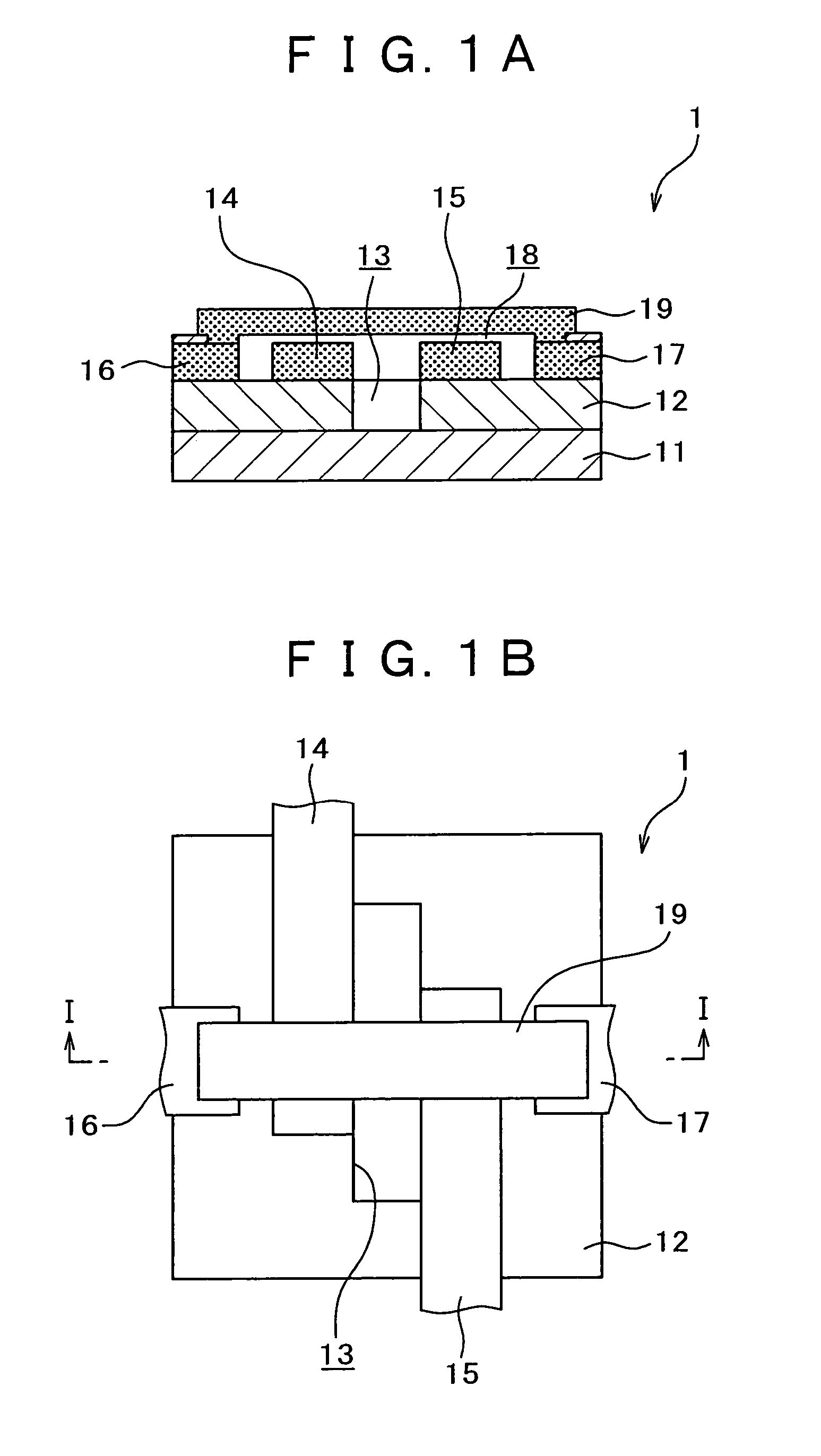
[0023]the micromachine of the present invention will be described referring to FIGS. 1A and 1B. FIG. 1A is a sectional view of the overall configuration, and FIG. 1B is a plan view, where FIG. 1A is a sectional view taken along a line I—I in FIG. 1B.
[0024]As shown in FIGS. 1A and 1B, an insulating layer 12 is formed on a substrate 11. The substrate 11 is a semiconductor substrate, for which a silicon substrate or compound semiconductor substrate, for example, can be used. The insulating layer herein is formed typically using a silicon nitride film, where it is also allowable to adopt a stacked structure of a silicon oxide film and a silicon nitride film, or a silicon oxide film depending on materials composing sacrificial layers described later with respect to the fabrication method. The insulating layer 12 has a groove 13 formed therein. For a case where the insulating layer 12 is composed of a stacked structure, a surface of the groove 13 is preferably composed of a film same as t...
second embodiment
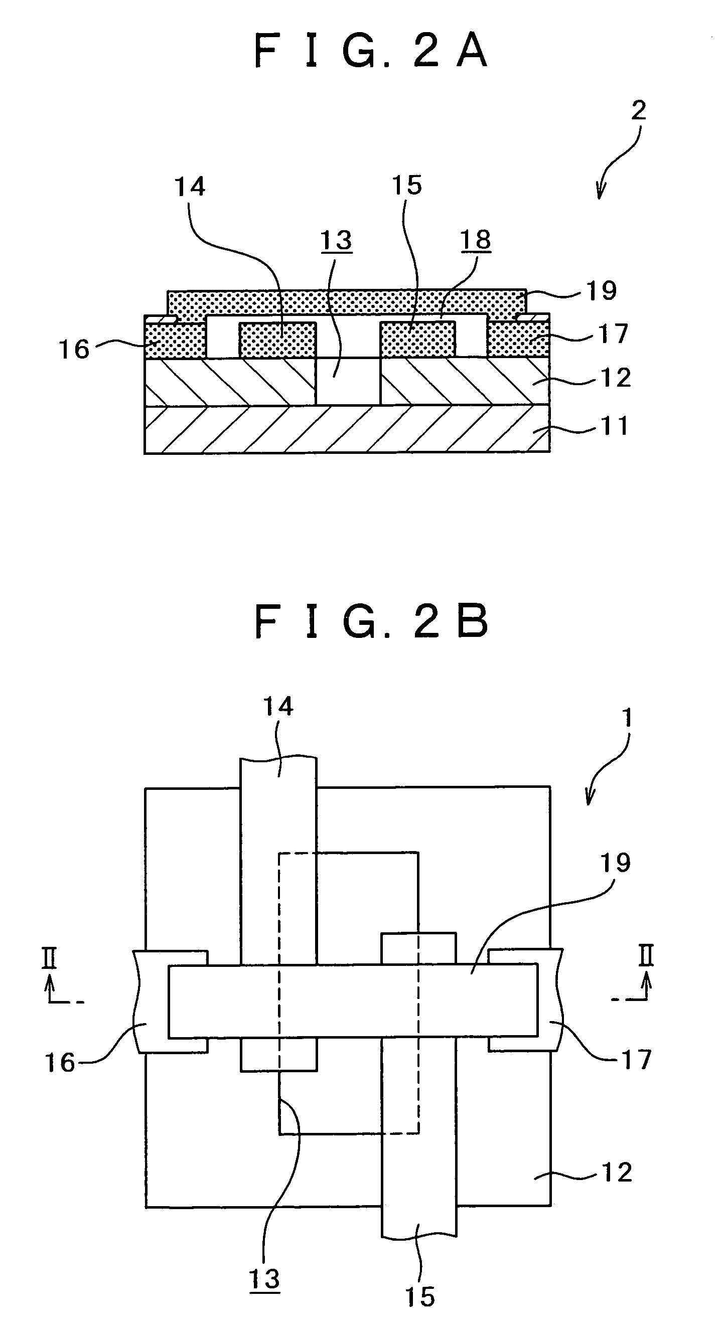
[0029]Next, the micromachine of the present invention will be described referring to FIGS. 2A and 2B. FIG. 2A is a sectional view of the overall configuration, and FIG. 2B is a plan view, where FIG. 2A is a sectional view taken along a line II—II in FIG. 2B.
[0030]As shown in FIGS. 2A and 2B, the insulating layer 12 is formed on the substrate 11. The substrate 11 is a semiconductor substrate, for which a silicon substrate or a compound semiconductor substrate, for example, can be used. The insulating layer 12 herein is formed typically using a silicon nitride film, where it is also allowable to adopt a stacked structure of a silicon oxide film and a silicon nitride film, or a silicon oxide film depending on materials composing sacrificial layers described later in relation to the fabrication method. The insulating layer 12 has the groove 13 formed therein.
[0031]The first electrode 14 for signal input (typically a signal input of a predetermined frequency, such as high-frequency signa...
third embodiment
[0035]Next, the micromachine of the present invention will be described referring to FIGS. 3A and 3B. FIG. 3A is a sectional view of the overall configuration, and FIG. 3B is a plan view, where FIG. 3A is a sectional view taken along a line III—III in FIG. 3B.
[0036]As shown in FIGS. 3A and 3B, the insulating layer 12 is formed on the substrate 11. The substrate 11 is a semiconductor substrate, for which a silicon substrate or compound semiconductor substrate, for example, can be used. The insulating layer 12 herein is formed typically using a silicon nitride film, where it is also allowable to adopt a stacked structure of a silicon oxide film and a silicon nitride film, or a silicon oxide film depending on materials composing sacrificial layers described later in relation to the fabrication method. The insulating layer 12 has the groove 13 formed therein. The groove 13 is formed in the insulating layer 12 so as to extend around the side edges of the first electrode 14 and the second...
PUM
| Property | Measurement | Unit |
|---|---|---|
| resonance frequency | aaaaa | aaaaa |
| DC voltage | aaaaa | aaaaa |
| thickness | aaaaa | aaaaa |
Abstract
Description
Claims
Application Information


