Semiconductor package having optimal interval between bond fingers for reduced substrate size

a technology of semiconductor chips and bond fingers, applied in the direction of semiconductor devices, semiconductor/solid-state device details, electrical equipment, etc., can solve the problems of difficult manufacturing of chips, wire bonding defects, and substantially impossible to design a substrate on which the semiconductor chip is mounted, so as to reduce the size of the substrate

Inactive Publication Date: 2008-01-03
SK HYNIX INC
View PDF6 Cites 4 Cited by
  • Summary
  • Abstract
  • Description
  • Claims
  • Application Information

AI Technical Summary

Benefits of technology

[0007]Embodiments of the present invention are directed to a semiconductor package in which an interval between bond fingers is increased while the size of a substrate is decreased.

Problems solved by technology

Consequently, it is difficult to manufacture a chip scale package of a size that is only 100% to 120% of the size of a semiconductor chip, thereby retrogressing the trend of increasingly slimmer semiconductor packages.
Meanwhile, decreasing the interval between bond fingers in order to prevent the size of a semiconductor package from increasing results in wire bonding defects, arising from the process of connecting the bonding pads of a semiconductor chip to the bond fingers of a substrate using wires, and testing defects, arising from the process of testing the semiconductor package.
As a result, as the number of bonding pads arranged on the surface of a semiconductor chip continually increases, it becomes substantially impossible to design a substrate on which the semiconductor chip is mounted, whereby the semiconductor chip cannot be appropriately packaged.

Method used


Image

  • Semiconductor package having optimal interval between bond fingers for reduced substrate size
  • Semiconductor package having optimal interval between bond fingers for reduced substrate size
  • Semiconductor package having optimal interval between bond fingers for reduced substrate size

Examples


first embodiment

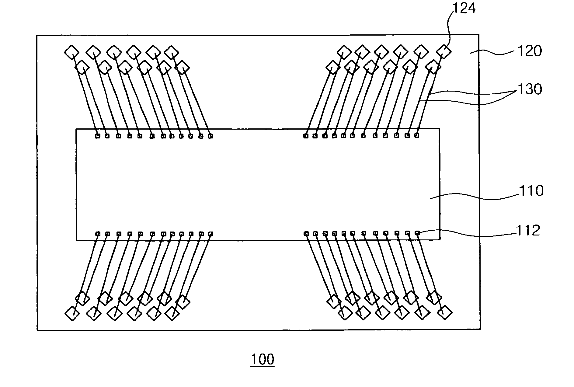
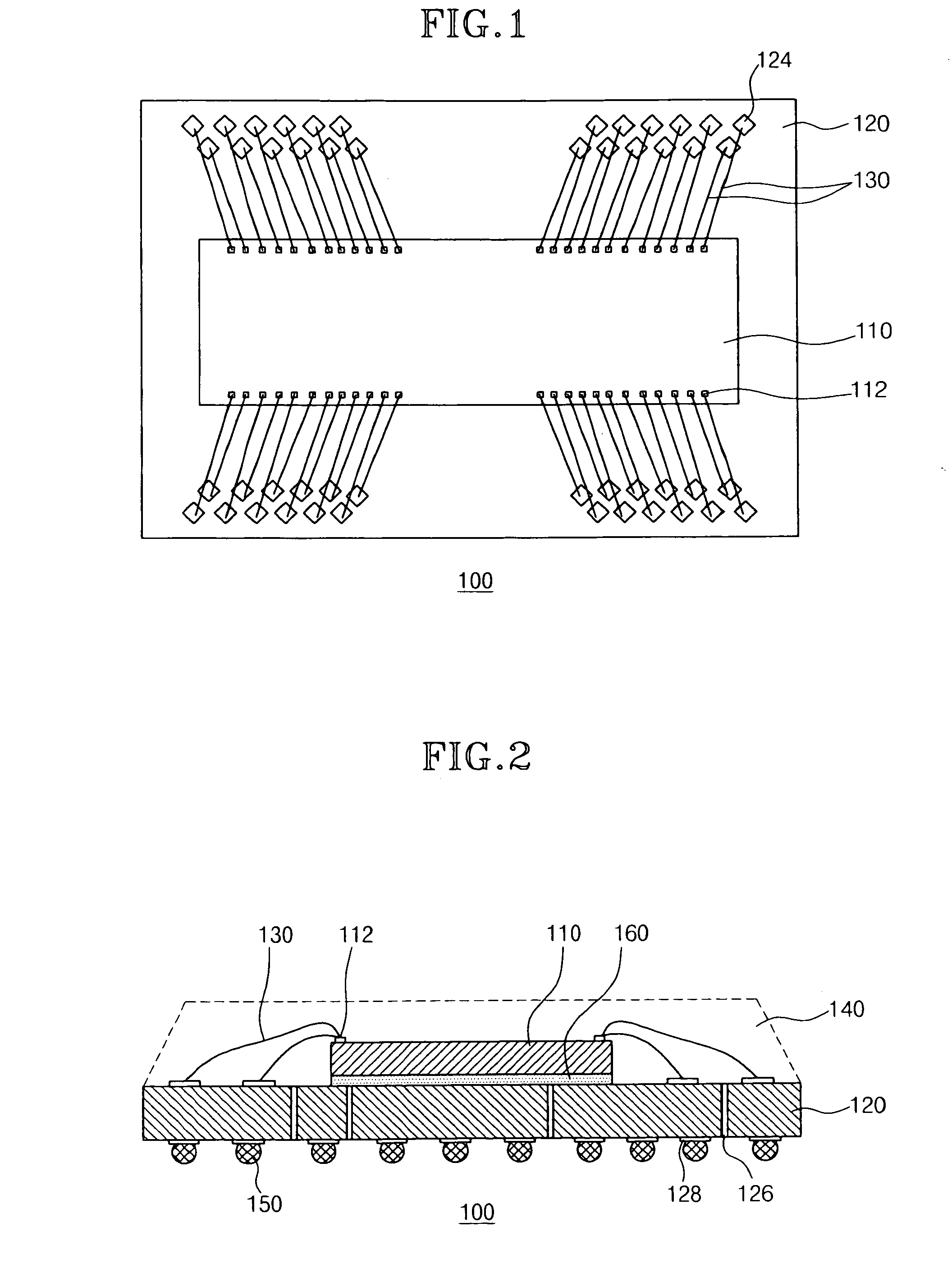
[0026]Referring to FIGS. 1 and 2, a semiconductor package 100 in accordance with the present invention includes a semiconductor chip 110, a substrate 120, wires 130, a molding material 140, and solder balls 150.

[0027]The semiconductor chip 110 has a circuit section (not shown) for storing various information inputted from the outside and a plurality of bonding pads 112, which are arranged on the upper surface of the semiconductor chip 110 and are electrically connected to the circuit section. In FIGS. 1 and 2, the bonding pads 112 are arranged in a row adjacent to each widthwise edge of the semiconductor chip 110. However, it is to be readily understood that the bonding pads 112 can be arranged in a row or a plurality of rows along the widthwise center portion of the semiconductor chip 110 or adjacent to the four edges of the semiconductor chip 110.

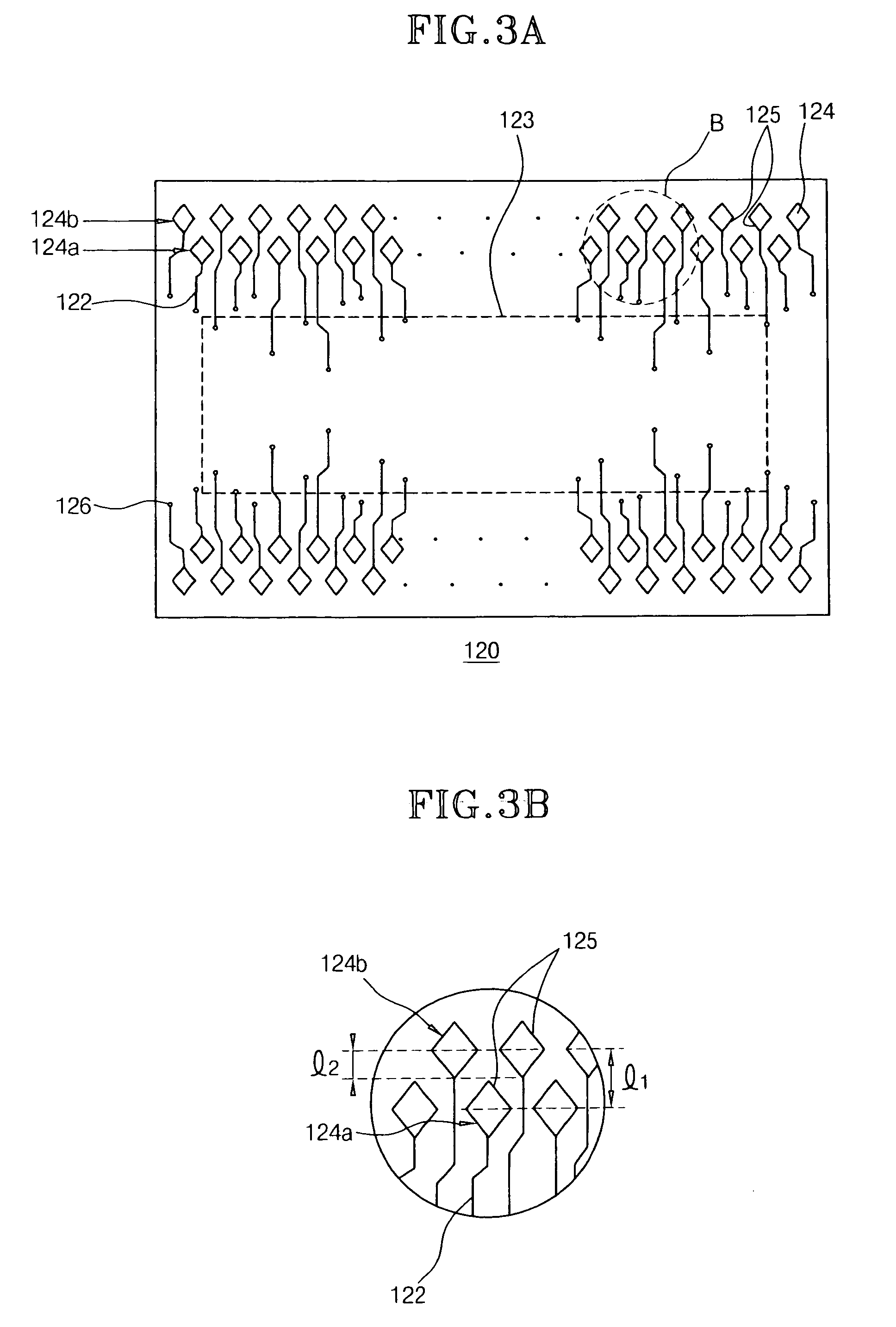
[0028]Referring to FIGS. 1 and 3A, the substrate 120 comprises a printed circuit board on which circuit patterns 122 are printed. The se...

second embodiment

[0042]FIGS. 6A through 6C are views for explaining a semiconductor package in accordance with the present invention, wherein FIG. 6A is a cross-sectional view illustrating the semiconductor package, FIG. 6B is a plan view illustrating the semiconductor chip of the semiconductor package, and FIG. 6C is a plan view illustrating the substrate of the semiconductor package.

[0043]Referring to FIG. 6A, the semiconductor package 600 in accordance with the second embodiment of the present invention has a configuration in which a semiconductor chip 610 and a substrate 620 are connected to each other not by wires but by conductive materials, namely solder bumps 660. In other words, in the semiconductor package 600 in accordance with this second embodiment of the present invention, after the solder bumps 660 are respectively formed on the bonding pads 612 of the semiconductor chip 610, the semiconductor chip 610 is attached to the substrate 620 using the solder bumps 660, such that the electric...


PUM


Abstract

A semiconductor package includes a semiconductor chip having a plurality of bonding pads, and a substrate having a first surface on which a plurality of bond fingers are arranged and a second surface on which ball lands connected to the bond fingers are formed. The bond fingers are arranged in a plurality of rows, and are formed in the shape of a polygon, such that overlapping surfaces of a bond finger of a row, which overlap with another bond finger of another row, have a constant slope, and overlapping surfaces of bond fingers arranged in the same row, which face each other, are sloped in opposite directions. Bond fingers of each row are positioned between the overlapping surfaces of bond fingers of another row, which face each other, such that the bond fingers of the rows are arranged in a zigzag pattern.

Description

CROSS-REFERENCE TO RELATED APPLICATIONS[0001]The present application claims priority to Korean patent application number 10-2006-0059812 filed on Jun. 29, 2006, which is incorporated by reference in its entirety.BACKGROUND OF THE INVENTION[0002]The present invention relates to a semiconductor package, and more particularly, to a semiconductor package in which an interval between bond fingers connected to a semiconductor chip is increased while the size of a substrate is decreased.[0003]In order to effect miniaturization, slimness and multiple functionalities of electronic appliances, new types of semiconductor packages, such as a chip scale package having a size corresponding to only 100% to 120% of the size of a semiconductor chip and a stack package having semiconductor chips stacked on one another, have been developed in the art.[0004]As multiple functionalities are continuously demanded of electronic appliances and wherefore semiconductor chips are highly integrated, the number ...

Claims


Application Information

Patent Timeline
Patent Type & Authority Applications(United States)
IPC IPC(8): H01L23/02
CPCH01L23/3121H01L2224/16225H01L24/06H01L24/49H01L2224/05552H01L2224/05553H01L2224/05599H01L2224/16H01L2224/48091H01L2224/49171H01L2224/49175H01L2224/49433H01L2224/85399H01L2924/01005H01L2924/014H01L2924/15311H01L23/49838H01L2224/32225H01L2224/48227H01L2224/73204H01L2224/73265H01L24/48H01L2924/00014H01L2924/01033H01L24/83H01L2224/0401H01L2224/83H01L2224/45099H01L2924/00H01L2924/00012H01L24/73H01L2224/05554H01L2924/10161H01L2924/181
Inventor PARK, JEONG HYUN
Owner SK HYNIX INC
Why Eureka
Try Eureka