Power module package structure

a power module and package technology, applied in the direction of semiconductor devices, semiconductor/solid-state device details, electrical apparatus, etc., can solve the problems of affecting the life and performance of electrical products, the package structure produces a lot of heat, and the cost is higher, so as to improve the heat transmission and circuit density, improve the heat transmission path, and increase the circuit density

Active Publication Date: 2006-11-30
CYNTEC
View PDF9 Cites 3 Cited by
  • Summary
  • Abstract
  • Description
  • Claims
  • Application Information

AI Technical Summary

Benefits of technology

[0009] In view of foregoing mentioned problems, one object of the present invention is to provide a power module package structure with a stacking structure and a good path for heat transmitting. The stacking structure is formed by stacking the circuit plate on the lead frame. And all circuits in the power module package structure are fabricated on the circuit plate. Therefore, the package structure improves the heat transmitting and the density of the circuits caused by the package structure in prior art.
[0010] Another object of the present invention is to provide a power module package structure with a circuit plate on which all circuit are fabricated thereon instead of on the substrate, as well as a stacking structure for increasing the density of the circuits and shrinking the size of the package. And the stacking structure is formed by stacking the circuit plate on part of the lead frame. Therefore, the size of the substrate is shrunk and the cost is reduced.
[0011] Yet another object of the present invention is to provide a power module package structure in which the power elements are disposed on a high thermal conduction material on the substrate or disposed on a high thermal conduction substrate directly. The heat produced by the power elements is transmitted from high thermal conduction material to outside through the substrate, but not the package material with low thermal conduction. So the rate of thermal conduction of this power module package structure is better than the rate of thermal conduction of the conventional power module package structure. The power module package structure can bear the passing of the heat produced by the passing of lots of electric currents in short time because its high rate of thermal conduction. So the power module will not be broken down by the heat.
[0012] Accordingly, one embodiment of the present invention provides a power module package structure with high density and high thermal condition. The package structure comprises a substrate with high thermal condition, and a lead frame is disposed on topside of the substrate. A circuit plate with all circuits of the power module is disposed on the part of the lead frame to form a stacking structure. There are one or several control elements disposed on the circuit plate. And several power elements are disposed on the high thermal conduction material like lead frame or metal block on the substrate, or are directly disposed on the substrate with high thermal conduction. There is a good heat transmitting path to be formed by both of the two ways. And several wire bonds are formed to connect to the circuit plate and the lead frame, the circuit plate and the power elements, the power elements and the lead frame. Part of the substrate-all elements-lead frame and circuit plate are encapsulated by a package material.
[0013] According to foregoing package structure, the size of the substrate become smaller because the circuits are fabricated on the circuit plate in stead of on the substrate, and the stacking structure formed by the lead frame and the substrate. By this way, the size of the package structure can be shrunk effectively. The power elements are disposed on the high thermal conduction substrate or on the high thermal material on substrate to form a good thermal condition path. Therefore, the heat produced by the power elements is transmitted to outside or heat sink effectively and quickly.

Problems solved by technology

However, lots of heat is produced by the package structure with the high integration of electrical elements and wire bonds, when the electrical products are working.
Especially for the power module, the heat affects the life and performance of the electrical product.
So this package structure needs a bigger substrate, and it's cost is higher because it's bigger substrate.
Although there are many advantages of this package structure in FIG. 2, but the density of the circuits still can not be increased because all circuits are fabricated on the substrate 100.
The density and accuracy of the circuits and package structure are limited because the circuits are fabricated on the lead frame.
But the heat is not transmitted very well.
It is because the heat is still transmitted from substrate to heat sink through the adhesive, and the adhesive is not a good thermal conductor.

Method used


Image

  • Power module package structure
  • Power module package structure
  • Power module package structure

Examples


Embodiment Construction

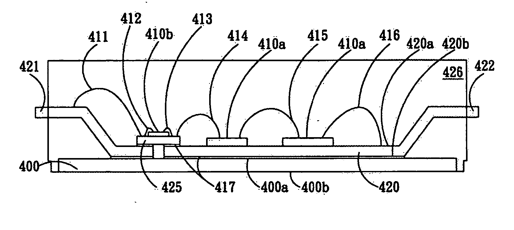
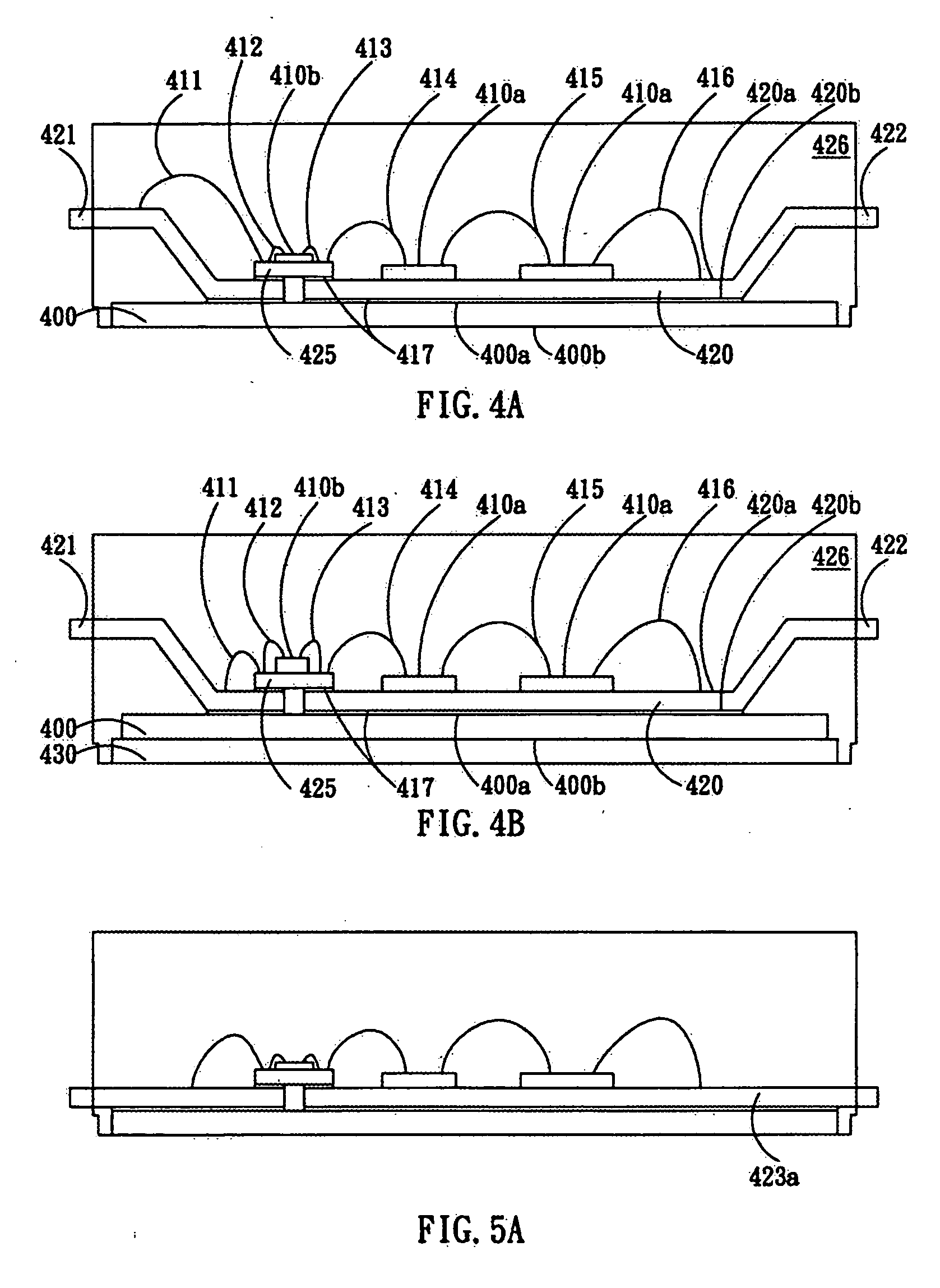
[0021] Referring to FIG. 4A, it is a cross-sectional diagram illustrating a power module package structure in accordance with one embodiment of the present invention. The package structure includes a substrate 400 with high thermal conduction and good isolation. There are a topside 400a and a backside 400b opposite to the topside 400a on the substrate 400. A lead frame 420 with several leads 421-422 and etc.(not show in the diagram) is disposed on the topside 400a of the substrate 400 by the second side 420b of the lead frame. A circuit plate 425 is disposed on the first side 420a of the lead frame 420 by connecting two of the ends of the circuit plate 425 with the first side 420a. A stacking structure is formed on the substrate 400 by this connecting. Therefore, the size of the substrate for package is effectively shrunk by this stacking structure. And the size of the package structure is also effectively shrunk by this stacking structure. Furthermore, one or a plurality of the sec...


PUM

PropertyMeasurementUnit
stacking structureaaaaaaaaaa
heat dispersion efficiencyaaaaaaaaaa
sizeaaaaaaaaaa

Abstract

A power module package structure is disclosed. The control circuits are fabricated on a circuit plate, instead of fabricating them directly on a main substrate. The fabrication cost is reduced because the size of the substrate is shrunk. Furthermore, the power chips are placed on a material with high thermal conductivity. The heat produced from the power chips can be transmitted quickly. Thus, the reliability of the power module package can be improved.

Description

BACKGROUND OF THE INVENTION [0001] 1. Field of the Invention [0002] The present invention generally relates to a kind of power module package structure. In particular, the present invention relates to a kind of power module package with characteristics of high heat dispersion efficiency and high integration. [0003] 2. Description of the Prior Art [0004] Increasing device complexity but shrinking size is common trend of the electrical product. Therefore, in addition to the shrinking size of the electrical product, how to put the most of electrical elements and wire bonds into the semiconductor package of the electrical product is very important. However, lots of heat is produced by the package structure with the high integration of electrical elements and wire bonds, when the electrical products are working. Especially for the power module, the heat affects the life and performance of the electrical product. Therefore, it is an important subject to improve the heat dispersion of the ...

Claims


Application Information

Patent Timeline
Patent Type & Authority Applications(United States)
IPC IPC(8): H01L23/34
CPCH01L2924/01033H01L2924/01013H01L24/48H01L2924/01002H01L23/49575H01L2924/014H01L2924/01006H01L2224/48227H01L2224/48137H01L2224/49H01L2924/01047H01L2224/48145H01L2224/48091H01L23/49531H01L24/49H01L2924/01004H01L23/4334Y10T29/49121Y10T29/49126H01L2924/19107H01L2924/01082H01L2924/00014H01L2924/181H01L2224/45099H01L2924/00012H01L23/02H01L25/10H01L23/48H01L23/36
Inventor LIU, CHUN-TIAOCHEN, DA-JUNGLIN, CHUN-LIANGLI, JENG-JENHSU, CHENG CHIEHWEN, CHAU CHUN
Owner CYNTEC
Why Eureka
Try Eureka