Adjustable thickness thermal interposer and electronic package utilizing same

a technology of thermal interposer and electronic package, which is applied in the direction of cooling/ventilation/heating modification, semiconductor/solid-state device details, semiconductor devices, etc., can solve the problems of difficult control of the dimensions of variations of such components, inefficient heat escape, and deleterious effects on chip operation and life, etc., to achieve excellent heat path for heat generated, high heat efficient path of heat dissipation

Inactive Publication Date: 2009-12-08
I3 ELECTRONICS
View PDF17 Cites 19 Cited by
  • Summary
  • Abstract
  • Description
  • Claims
  • Application Information

AI Technical Summary

Benefits of technology

[0022]It is another object of the invention to provide an electronic package with a thermal interposer which provides an excellent heat path for heat generated from an electronic component to the package's heat sink.
[0023]It is yet another object of the invention to provide such an electronic package which can be produced in a relatively inexpensive manner.
[0024]It is still another object of the invention to control force application and assure acceptable tolerance ranges during the assembly of electronic packages and the like while assuring a highly efficient path of heat dissipation for such packages.

Problems solved by technology

As is well known, inefficient heat escape can deleteriously affect the chip's operation and life.
The ability to control variations in the dimensions of such components is difficult, especially where the components come from different sources (vendors) or where reworking or modification of such components is required.
This problem is especially apparent where large scale commercial production is involved.

Method used


Image

  • Adjustable thickness thermal interposer and electronic package utilizing same
  • Adjustable thickness thermal interposer and electronic package utilizing same
  • Adjustable thickness thermal interposer and electronic package utilizing same

Examples


Embodiment Construction

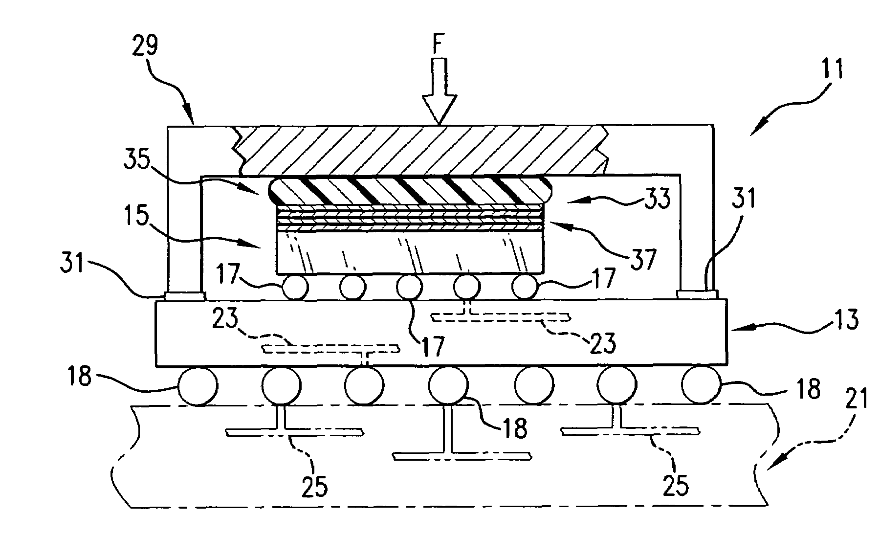
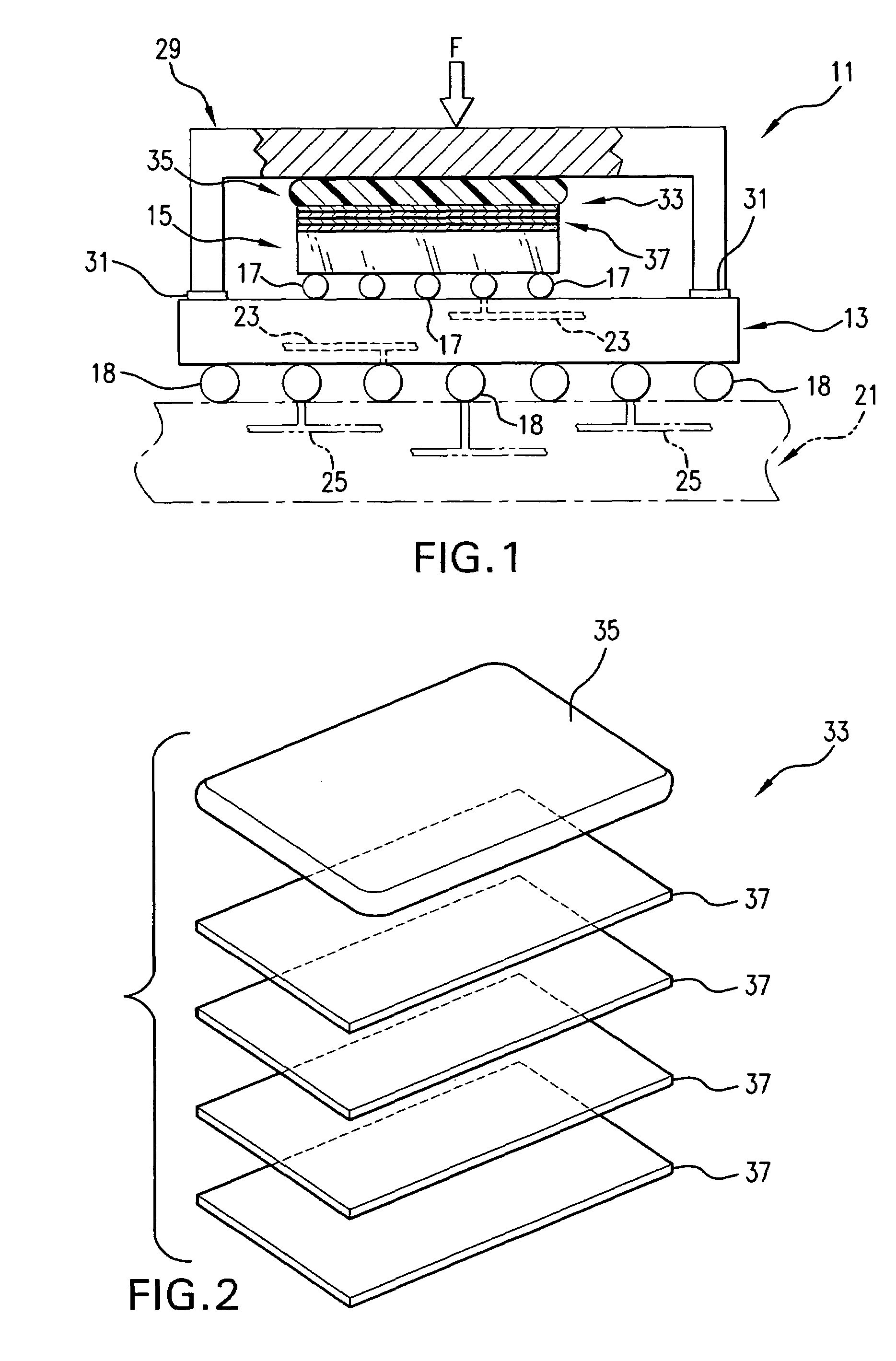
[0031]For a better understanding of the present invention, together with other and further objects, advantages and capabilities thereof, reference is made to the following disclosure and appended claims in connection with the above-described drawings. It is understood that like numerals will be used to indicate like elements from FIG. to FIG.

[0032]By the term “circuitized substrate” as used herein is meant to include substrates having at least one (and preferably more) dielectric layer(s) and at least one (and preferably more) metallurgical conductive layer(s). Examples include structures made of dielectric materials such as fiberglass-reinforced epoxy resins (some referred to as “FR-4” dielectric materials in the art), polytetrafluoroethylene (Teflon), polyimides, polyamides, cyanate resins, photo-imagable materials, alumina ceramics, glass ceramics, low temperature co-fired ceramics, and other like materials wherein the conductive layers are each a metal layer (e.g., power, signal...


PUM


Abstract

An electronic package which includes a substrate (e.g., a chip carrier substrate or a PCB), an electronic component (e.g., a semiconductor chip), a heatsink and a thermal interposer for effectively transferring heat from the chip to the heatsink. The interposer includes a compressible, resilient member (e.g., an elastomeric pad) and a plurality of thin, metallic sheets (e.g., copper foils) and the thickness thereof can be adjusted by altering the number of such foils.

Description

TECHNICAL FIELD[0001]The present invention relates to structures and methods for controlling the thickness of the gap between a semiconductor chip and a lid, heatsink (also referred to herein as a heat sink), or other cooling mechanism designed to provide cooling for the chip. More particularly, the present invention is directed to an assembly (interposer) in which the size of the gap (thickness) between the chip and the cooling mechanism is controlled, preferably so that the gap is as small as possible without deleteriously affecting the assembly process, chip integrity, or assembly performance.BACKGROUND OF THE INVENTION[0002]Electronic packages (sometimes called modules) including semiconductor chips, especially high power chips, demand that heat from the chip be effectively dissipated away from the chip to the environment external of the package. The ability of the package to dissipate heat generated by the chip(s) is generally a function of the quality of the primary heat dissi...

Claims


Application Information

Patent Timeline
Patent Type & Authority Patents(United States)
IPC IPC(8): H01L23/34
CPCH01L23/3735H01L23/433H01L24/31H01L23/3737H01L2224/32245H01L2224/16225H01L2224/73253H01L2924/01005H01L2924/01013H01L2924/01027H01L2924/01029H01L2924/01042H01L2924/01047H01L2924/01049H01L2924/01074H01L2924/01079H01L2924/09701H01L2924/14H01L2924/15311H01L2924/16152H01L2924/3011H01L2924/01006H01L2924/01033H01L2924/01087H01L2224/16227
Inventor ALCOE, DAVID J.CALMIDI, VARAPRASAD V.
Owner I3 ELECTRONICS
Why Eureka
Try Eureka