Multi-layer ceramic substrate with embedded cavity and manufacturing method thereof

a multi-layer ceramic and cavity technology, applied in the field of ceramic substrates, can solve the problems of circuits or the overall substrate deformation, increase the difficulty of circuit design and manufacturing processes, and solve problems such as circuit integration, circuit integration can be increased, and the substrate size can be reduced.

Inactive Publication Date: 2009-02-26
DELTA ELECTRONICS INC
View PDF0 Cites 1 Cited by
  • Summary
  • Abstract
  • Description
  • Claims
  • Application Information

AI Technical Summary

Benefits of technology

[0012]As mentioned hereinabove, the multi-layer ceramic substrate with the embedded cavity and the manufacturing method thereof according to the invention have the following features. First, the sintered ceramic thin plate and the non-sintered ceramic pre-mold plate are stacked and sintered so that the ceramic thin plate can provide a constraining action to the ceramic pre-mold plate to suppress the ceramic pre-mold plate from contraction during the sintering process. Thus, the sintering contraction in the plane direction can be avoided. Compared with the prior art, the ceramic thin plate and the ceramic pre-mold plate have the same property, the contraction can be suppressed during the sintering process, and it is possible to prevent the ceramic thin plate and the ceramic pre-mold plate from being curved so that the even ceramic substrate can be obtained. In addition, the embedded cavity is formed inside the ceramic substrate and electronic elements are placed into the embedded cavity so that the circuit integration can be increased and the size of the substrate can be reduced.

Problems solved by technology

However, there are some problems to be solved in the LTCC application.
The main drawback is the contraction caused by sintering the ceramic substrate, wherein the contraction in the plane direction has the greatest influence so that the circuits or the overall substrate may deform.
In addition, the ceramic substrates produced in different batches may also have different contraction rations, thereby increasing the difficulty in the circuit design and the manufacturing processes and thus restricting the application range thereof.
However, the manufacturing cost is increased, and the manufacturing processes become complicated.
The conventional ceramic substrate only has top and bottom surfaces, on which circuits may be formed or surface elements may be mounted, and thus cannot satisfy the miniaturized requirement.

Method used


Image

  • Multi-layer ceramic substrate with embedded cavity and manufacturing method thereof
  • Multi-layer ceramic substrate with embedded cavity and manufacturing method thereof
  • Multi-layer ceramic substrate with embedded cavity and manufacturing method thereof

Examples


Embodiment Construction

[0019]The present invention will be apparent from the following detailed description, which proceeds with reference to the accompanying drawings, wherein the same references relate to the same elements.

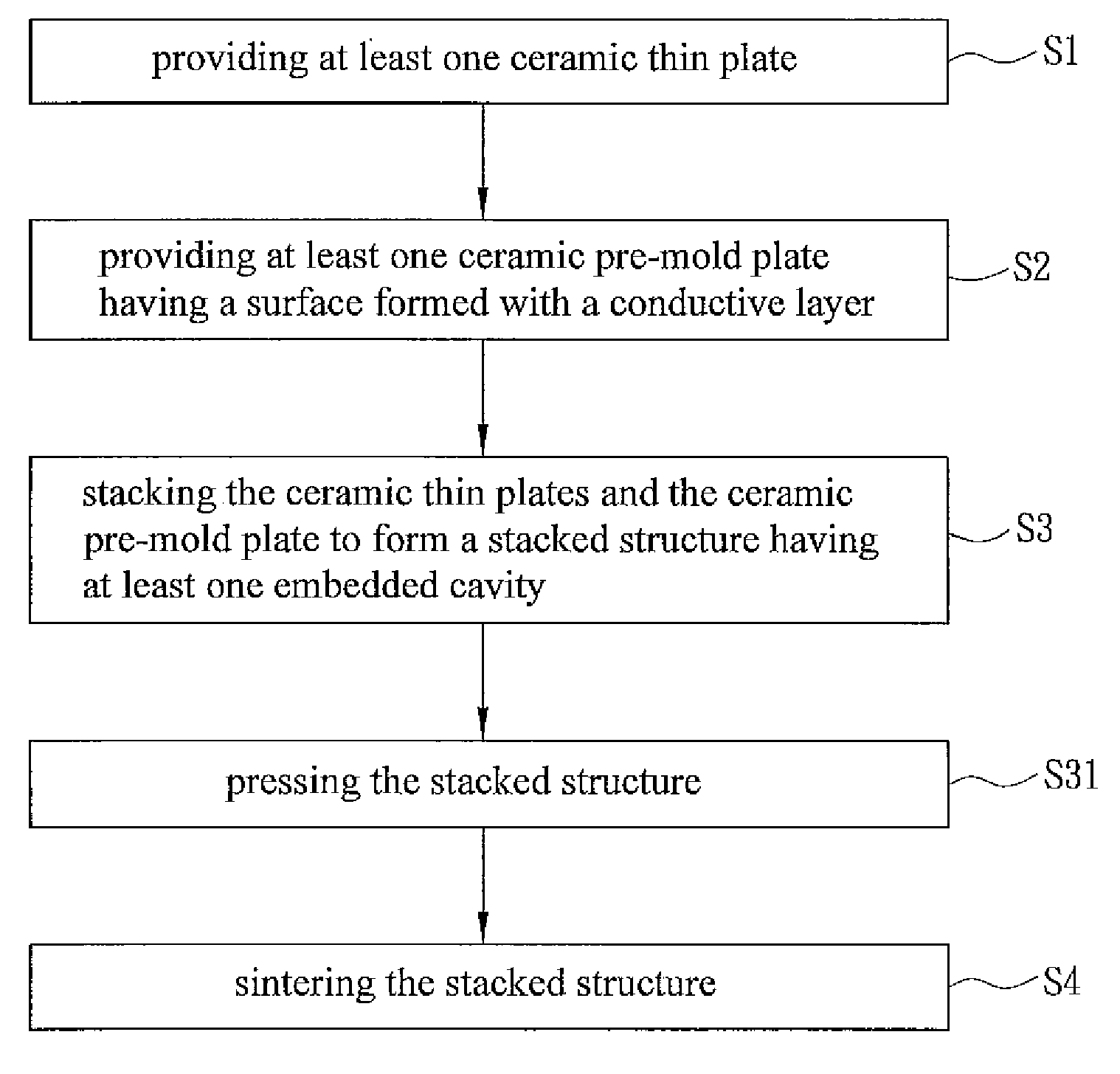
[0020]As shown in FIG. 1, a manufacturing method of a ceramic substrate according to a preferred embodiment of the invention includes steps S1 to S4.

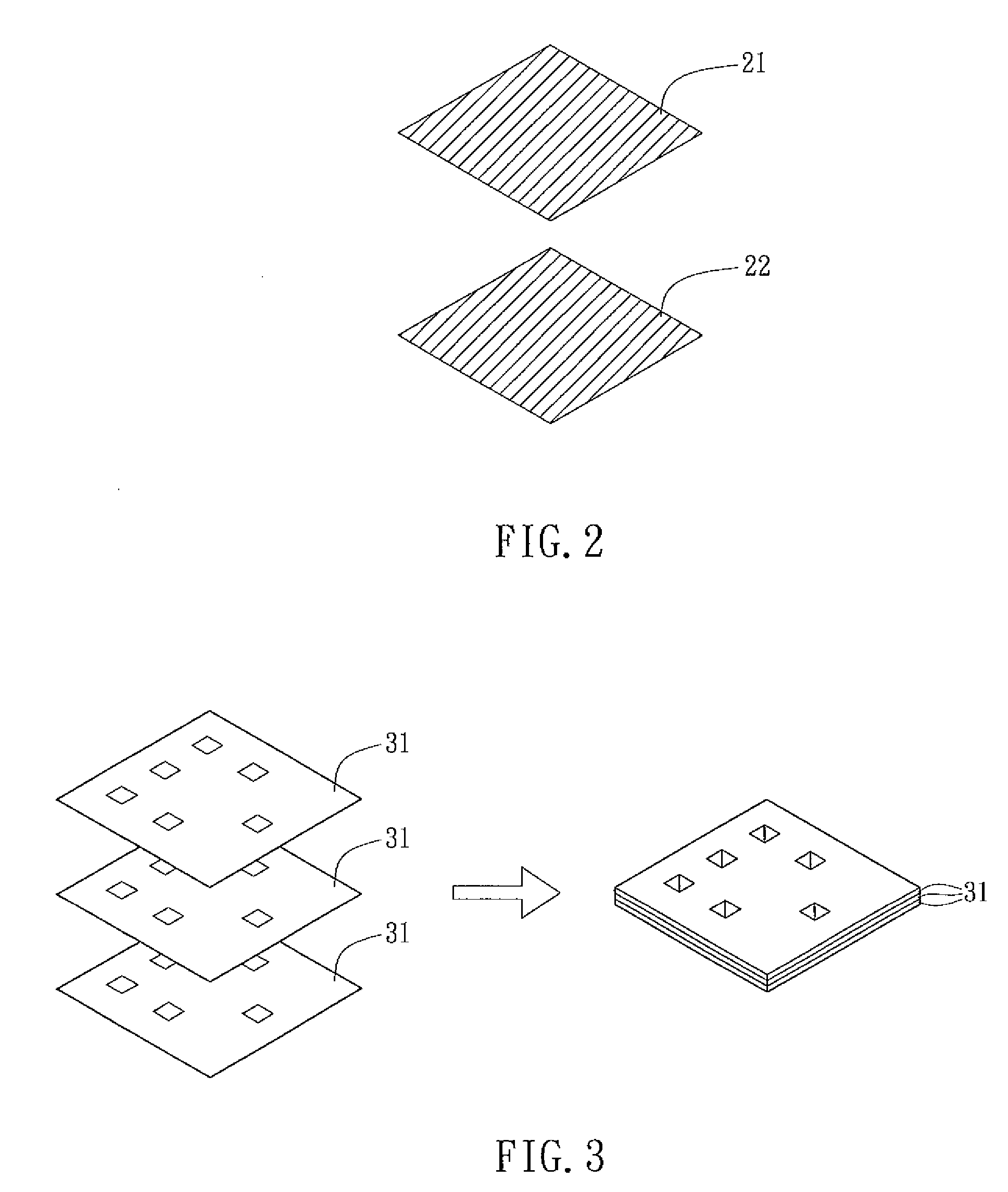
[0021]As shown in FIGS. 1 and 2, at least one ceramic thin plate is provided in the step S1. In this embodiment, two ceramic thin plates 21 and 22 are provided without any limitative purpose. The ceramic thin plates 21 and 22 may be prepared according to the following steps. First, a second pre-mold plate with a low sintering temperature interposed between two first pre-mold plates with high sintering temperatures. Next, the second pre-mold plate is sintered into the ceramic thin plates 21 and 22 at the low sintering temperature. During this sintering process, the first pre-mold plates provide a pressing action to the second pre-mold plat...


PUM

PropertyMeasurementUnit
conductiveaaaaaaaaaa
temperaturesaaaaaaaaaa
temperatureaaaaaaaaaa

Abstract

A multi-layer ceramic substrate with an embedded cavity and a manufacturing method thereof are disclosed. The method includes the steps of: providing at least one ceramic thin plate and at least one ceramic pre-mold plate having a surface formed with a conductive layer; stacking the ceramic thin plate and the ceramic pre-mold plate to form a stacked structure with at least one embedded cavity; and sintering the stacked structure.

Description

CROSS REFERENCE TO RELATED APPLICATIONS[0001]This Non-provisional application claims priority under 35 U.S.C. §119(a) on Patent Application No(s). 096131432 filed in Taiwan, Republic of China on Aug. 24, 2007, the entire contents of which are hereby incorporated by reference.BACKGROUND OF THE INVENTION[0002]1. Field of Invention[0003]The invention relates to a ceramic substrate and a manufacturing method thereof. More particularly, the invention relates to a multi-layer ceramic substrate with an embedded cavity and a manufacturing method thereof.[0004]2. Related Art[0005]At present, the electronic technology is rapidly developed, and the product is gradually miniaturized. Therefore, active and passive components are continuously developed in a direction toward the miniaturization. Due to the progress of the low-temperature co-fired ceramic technology (LTCC), the passive components can be integrated in a printing circuit ceramic substrate so that the area for the arrangement of the p...

Claims


Application Information

Patent Timeline
Patent Type & Authority Applications(United States)
IPC IPC(8): B32B17/06
CPCB32B18/00C04B2237/68H05K1/0272H05K1/0306H05K1/186H05K3/4611H05K3/4629H05K3/4697H05K2201/10636H05K2203/063C04B35/6455C04B37/001C04B37/042C04B2237/32C04B2237/34C04B2237/62Y02P70/50
Inventor WEI, CHIH HUNGHSIEH, YU PING
Owner DELTA ELECTRONICS INC
Why Eureka
Try Eureka