Non-volatile memory and fabricating method thereof

Inactive Publication Date: 2008-01-24
EMEMORY TECH INC
View PDF19 Cites 19 Cited by
  • Summary
  • Abstract
  • Description
  • Claims
  • Application Information

AI Technical Summary

Benefits of technology

[0042]In the method of fabricating non-volatile memory according to the present invention, a first conductive plug is formed on top of the floating gate to serve as an erase gate. Moreover, the specific dielectric layer (a self-aligned salicide block oxide or a resistive-protective oxide) is used as an inter-layer dielectric layer between the floating gate and the first conductive plug (the erase gate). The first conductive plug can be fabricated together with the second conductive plug and t

Problems solved by technology

On the other hand, with the ever-increasing amount of data that needs to be processed and saved by information electronic products (for example, computer, mobile phone, digital camera or personal digital assistant (PDA)), the required memory capacity of these information electronic products is becoming larger.
Hence, not only is the throughput of the fabrication process decreased, but also the fabrication cost is increased.
Because, electrons also pass through the tunnel dielectric layer into the floating gate or out of the floating gate when performing a programming operation or an erase operation of this typ

Method used


Image

  • Non-volatile memory and fabricating method thereof
  • Non-volatile memory and fabricating method thereof
  • Non-volatile memory and fabricating method thereof

Examples


Example

[0055]Reference will now be made in detail to the present preferred embodiments of the invention, examples of which are illustrated in the accompanying drawings. Wherever possible, the same reference numbers are used in the drawings and the description to refer to the same or like parts.

[0056]First, the non-volatile memory of the present invention is described.

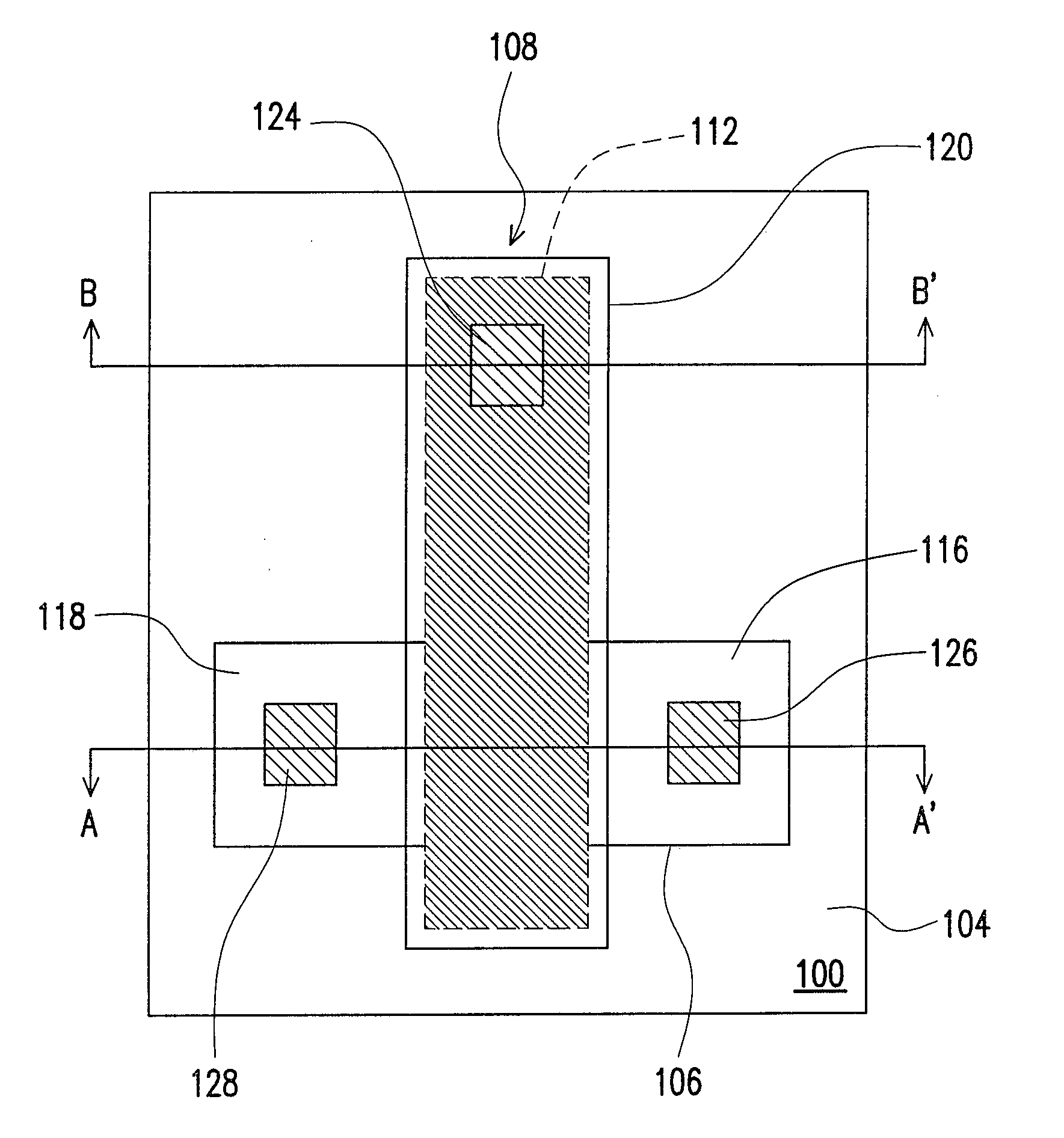
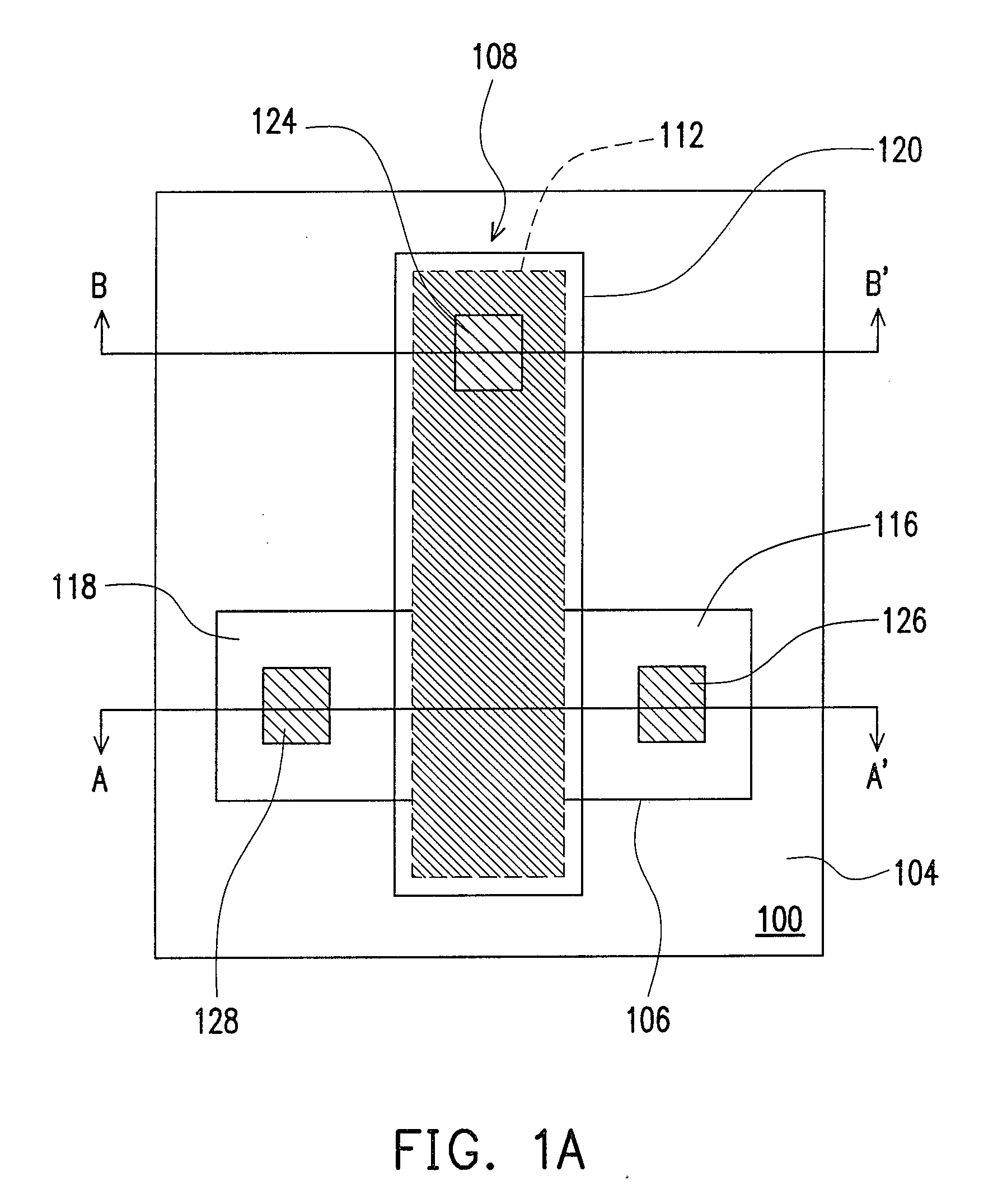
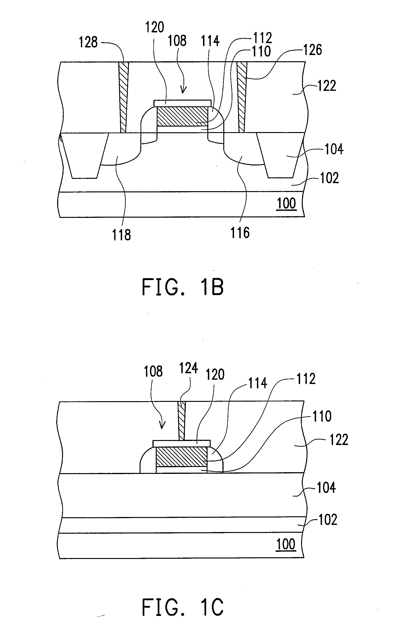
[0057]FIG. 1A is a top view of a non-volatile memory according to an embodiment of the present invention. FIG. 1B is a schematic cross-sectional view along line A-A′ of FIG. 1A. FIG. 1C is a schematic cross-sectional view along line B-B′ of FIG. 1A.

[0058]As shown in FIGS. 1A to 1C, the non-volatile memory of the present invention is disposed on a substrate 100, for example. The substrate 100 is a silicon substrate and has a well region 102, for example. Furthermore, the substrate 100 has an isolation structure 104 that defines an active region 106. The isolation structure 104 is, for example, a shallow trench isolation (STI) s...


PUM


Abstract

A non-volatile memory having an isolation structure, a floating gate transistor, a specific dielectric layer and an erase gate is provided. The isolation structure is disposed in a substrate to define an active region. The floating gate transistor having a floating gate, a tunneling dielectric layer, a first source/drain region and a second source/drain region is disposed on the substrate. The floating gate is disposed on the substrate and runs across the active region. The tunneling dielectric layer is disposed between the floating gate and the substrate. The first source/drain region and the second source/drain region are disposed in the substrate at the sides of the floating gate, respectively. The specific dielectric layer serves as an inter-layer dielectric layer, which is disposed on top of the floating gate. The erase gate is a conductive plug disposed upon the specific dielectric layer.

Description

CROSS-REFERENCE TO RELATED APPLICATION[0001]This application claims the priority benefit of U.S.A. provisional application Ser. No. 60 / 807,615, filed on Jul. 18, 2006, all disclosures are incorporated herein by reference.BACKGROUND OF THE INVENTION[0002]1. Field of the Invention[0003]The present invention generally relates to a semiconductor device, and more particularly, to a non-volatile memory and fabricating method thereof.[0004]2. Description of Related Art[0005]When semiconductor process proceeds into deep sub-micron regime, the dimension of devices is gradually reduced. For memory devices, this trend implies that the dimension of memory cells is becoming smaller. On the other hand, with the ever-increasing amount of data that needs to be processed and saved by information electronic products (for example, computer, mobile phone, digital camera or personal digital assistant (PDA)), the required memory capacity of these information electronic products is becoming larger. Subjec...

Claims


Application Information

Patent Timeline
IPC IPC(8): H01L29/788H01L21/3205
CPCH01L21/76829H01L27/115H01L29/7881H01L27/11558H01L29/66825H01L27/11521H10B69/00H10B41/30H10B41/60
Inventor LIN, CHRONG-JUNGCHEN, HSIN-MINGKING, YA-CHIN
Owner EMEMORY TECH INC
Why Eureka
Try Eureka