Method for fabricating a through hole on a semiconductor substrate

Active Publication Date: 2005-07-07
NEXCHIP SEMICON CO LTD
View PDF14 Cites 3 Cited by
  • Summary
  • Abstract
  • Description
  • Claims
  • Application Information

AI Technical Summary

Benefits of technology

[0010] It is an advantage of the claimed invention that the ARC layer is anteriorly etched before the dielectric layer is formed so that an etching agent having high etching selectivity to the ARC layer can be used to effectively remove the ARC layer. Accordingly, a thinner photoresist layer can be used as the etching mask in the second etching process for etching the dielectric layer because the longer etching process for etchi

Problems solved by technology

During a longer etching process, corners being cut or collapse

Method used


Image

  • Method for fabricating a through hole on a semiconductor substrate
  • Method for fabricating a through hole on a semiconductor substrate
  • Method for fabricating a through hole on a semiconductor substrate

Examples


Example

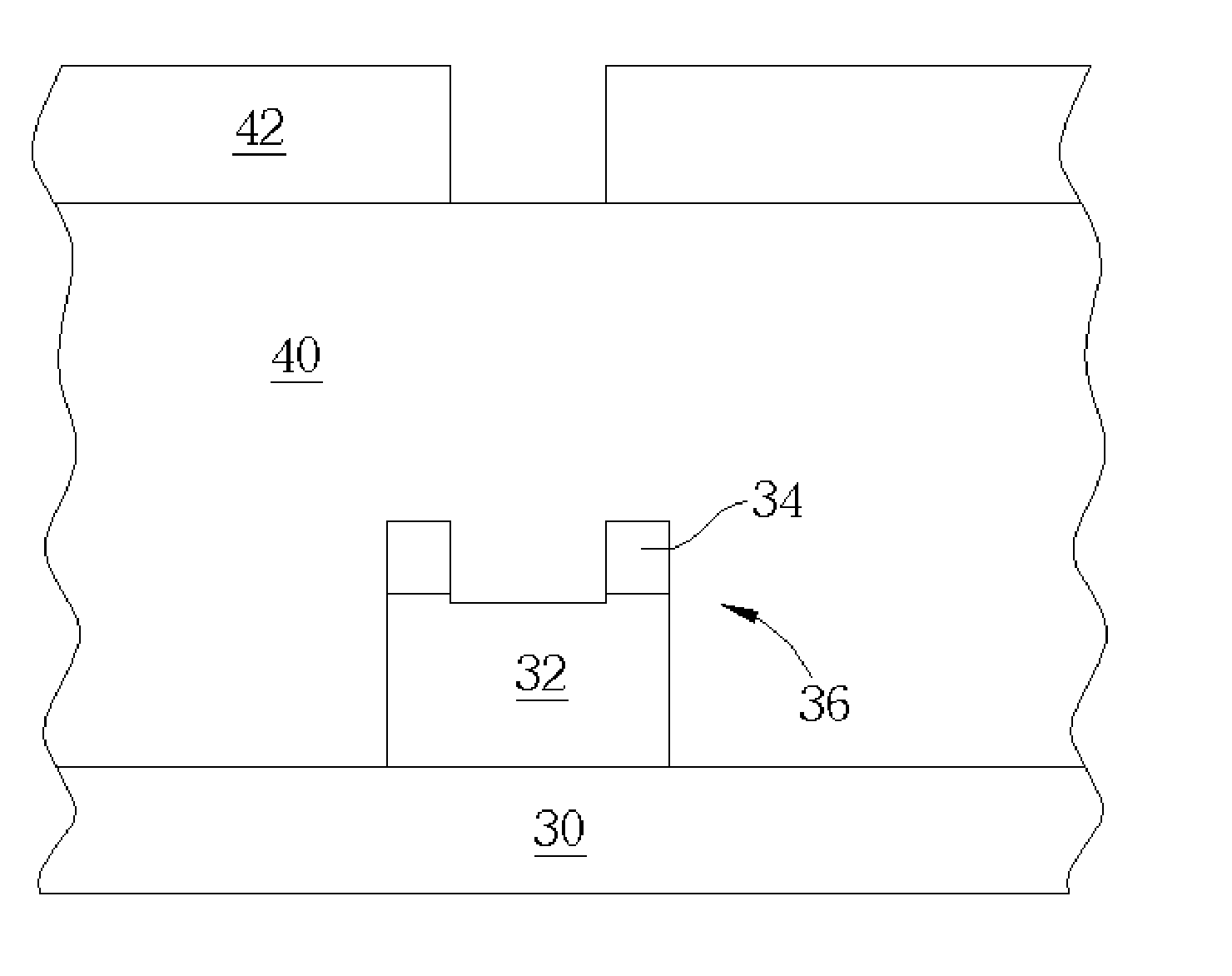
[0014] Please refer to FIGS. 4-10. FIGS. 4-10 are schematic diagrams of a method for fabricating at least a through hole on a substrate 30 according to the present invention. As shown in FIG. 4, a metal conductive layer 32 and an ARC layer 34 are formed on the surface of the substrate 30, wherein the substrate 30 may further have a plurality of prefabricated semiconductor elements and dielectric layers. The metal conductive layer 32 is composed of usual conductive materials of semiconductor process, such as aluminum alloy or aluminum copper alloy. The ARC layer 34 is used to reduce the high reflectivity of the metal conductive layer 32 to insure the accuracy and performance of the photolithography and etching process, and thereby the ARC layer 34 is composed of materials which can meet this requirement, such as TiN / Ti.

[0015] As shown in FIG. 5, a photolithography and etching process is performed to form a patterned photoresist layer (not shown) on the ARC layer 34 to define a condu...


PUM


Abstract

A method for fabricating a through hole is disclosed. First, a conductive structure having a conductive layer and a cap layer are formed on a substrate. A patterned first photoresist layer is formed on the substrate and the conductive structure to define a pattern of the through hole. Then, a first etching process to remove the cap layer not covered by the first photoresist layer is performed until the conductive layer is exposed. The first photoresist layer is removed. A dielectric layer and a patterned second photoresist layer are formed on the substrate. Finally, a second etching process is performed to remove the dielectric layer not covered by the second photoresist layer until the conductive layer is exposed. The pattern of the second photoresist layer is the same as the pattern of the first photoresist layer.

Description

BACKGROUND OF INVENTION [0001] 1. Field of the Invention [0002] The invention relates to a method for fabricating a through hole, and more particularly, to a method for fabricating a through hole by performing two etching processes. [0003] 2. Description of the Prior Art [0004] In semiconductor fabrication, in order to electrically connect device as metal oxide semiconductor (MOS) transistors with each metal conductive layer to form a complete electrical circuit, contact plugs and via plugs need to be formed in dielectric layers for serving as conductive lines of the MOS transistors and metal conductive layers when performing a multilevel metallization process. [0005] The conventional process for forming contact plugs and via plugs includes performing an etching process to form through holes, such as contact holes and via holes, in the dielectric layers, and filling with metal materials with low resistivity into the contact holes and via holes to form the contact plugs and the via p...

Claims


Application Information

Patent Timeline
IPC IPC(8): H01L21/4763H01L21/76H01L21/768H01L21/8242
CPCH01L21/76805H01L21/76802
Inventor TSENG, SHIEN CHUN
Owner NEXCHIP SEMICON CO LTD
Why Eureka
Try Eureka