

Method of manufacturing hybrid structure of multi-layer substrates and hybrid structure thereof
- Summary
- Abstract
- Description
- Claims
- Application Information
AI Technical Summary
Benefits of technology
Problems solved by technology
Method used
Image

Examples
second embodiment
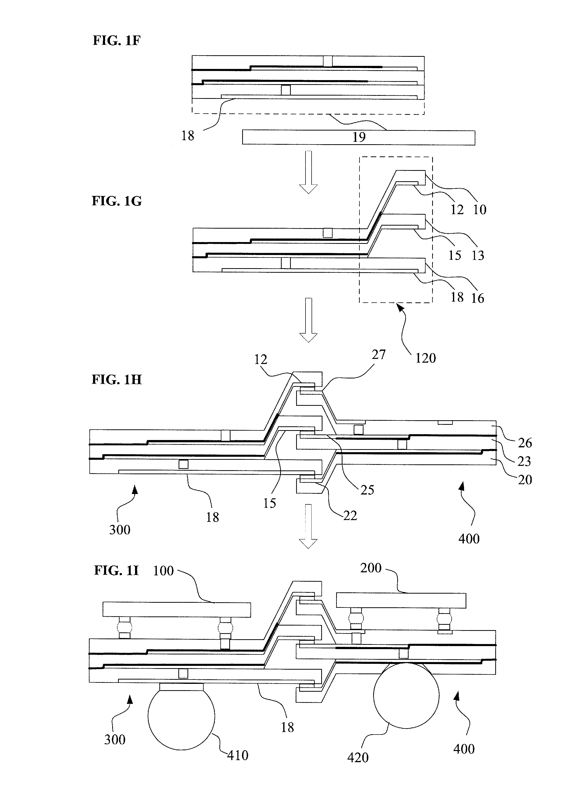
[0042]FIG. 2C shows step (c), in the second embodiment, an interface adhesion enhancing process is implemented on districts 17 to increase adhesion intensity between the first dielectric layer 16 and the first dielectric layer 19 coated in step (b) before coating the first dielectric layer 16. The aforesaid interface adhesion enhancing process can decrease the possibility that a separation between the dielectric layers 16, 19 or a deformation of the dielectric layers 16, 19 may happen and the dielectric layers 16, 19 may become unfit with each other during the coming step (d) shown in FIG. 2D, therefore, leading to an improved manufacturing the hybrid structure of multi-layer substrates.
[0043]Moreover, the sequence of the step (g) and the step (h) can be exchanged but there is no effect on the hybrid structure of multi-layer substrates of the present invention and the function thereof.
[0044]Please refer to FIG. 3A to FIG. 3H. FIG. 3C to FIG. 3H illustrate different step (c) to step ...
fourth embodiment
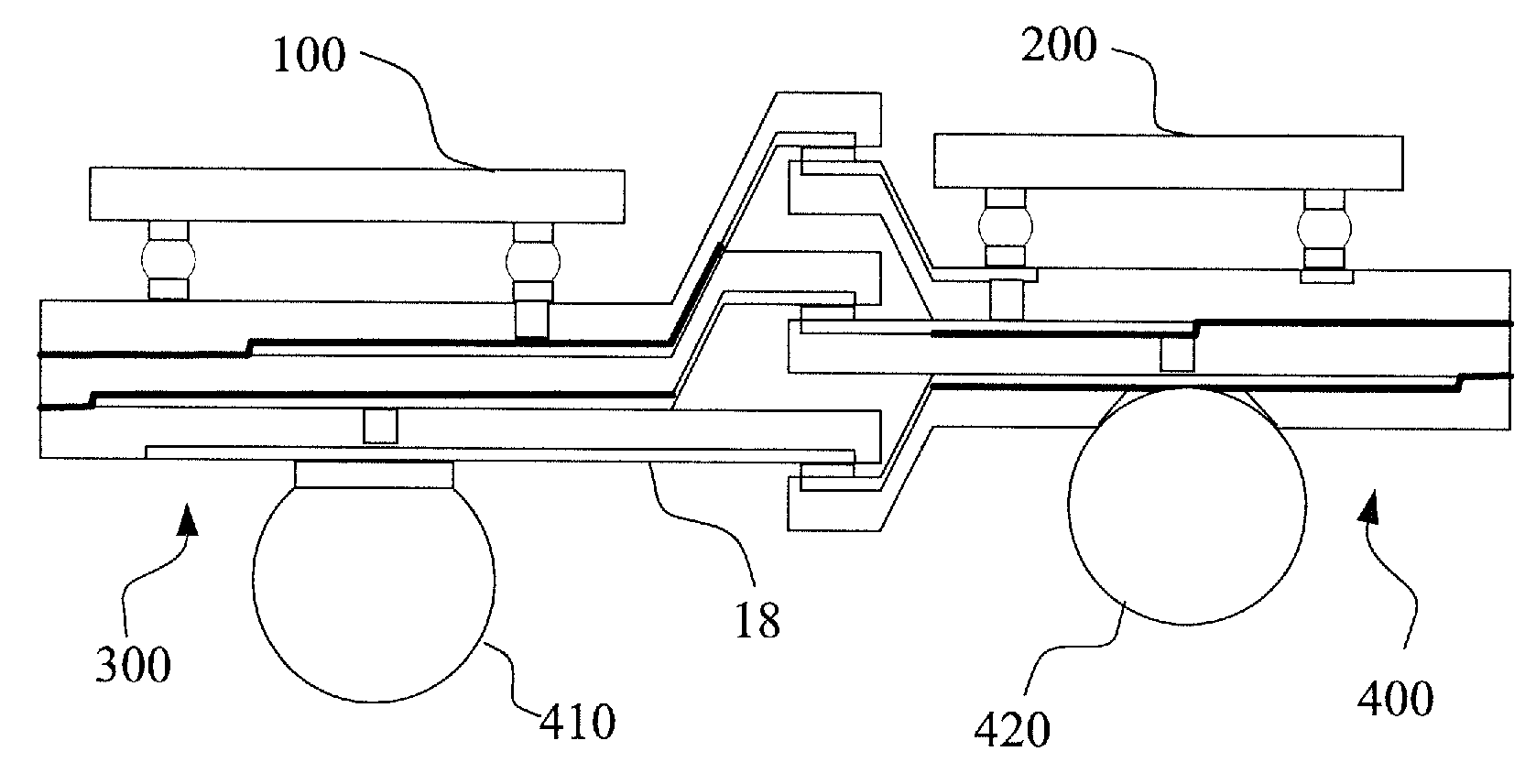
[0051]Please refer to FIG. 4A to FIG. 4I, which illustrate a flowchart of a method of manufacturing the hybrid structure of multi-layer substrates according to step (a) to step (h) in the present invention.
[0052]The method of manufacturing the hybrid structure of multi-layer substrates according to the fourth embodiment of the present invention comprises steps below:
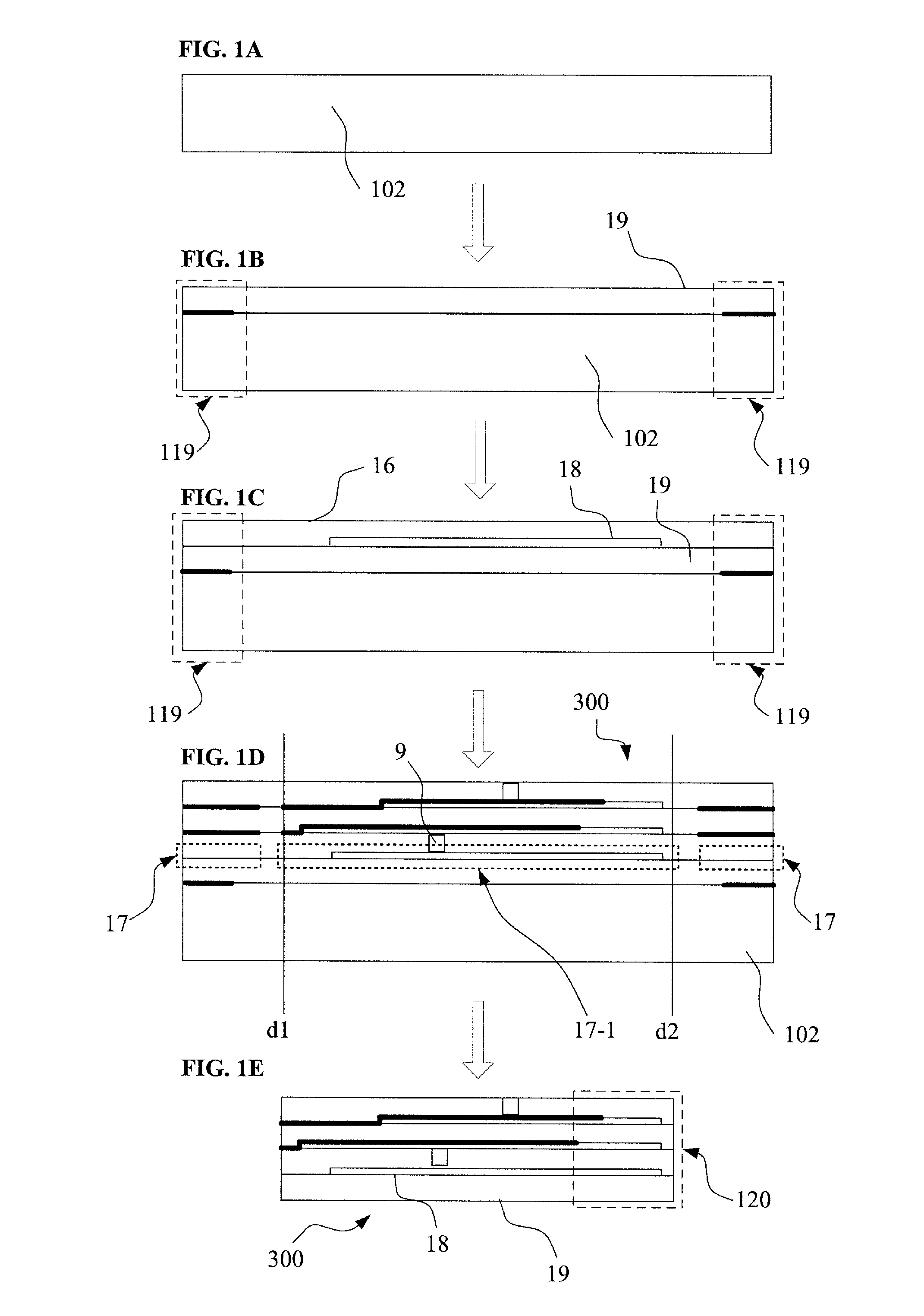
[0053]FIG. 4A shows step (a), providing a carrier 102 to form one of the multi-layer substrates (taking the first multi-layer substrate 300 for example) thereon;
[0054]FIG. 4B shows step (b), implementing an interlace adhesion enhancing process on the surface of the carrier 102 to increase adhesion intensity between the carrier 102 and a dielectric layer 104 and coating another dielectric layer 19 after hardening the dielectric layer 104;
[0055]FIG. 4C shows step (c), forming a necessary VIA 9 (shown in FIG. 1D) or more in the first dielectric layer 19 and a first metal layer 18 on the first dielectric layer 19 and then co...
fifth embodiment
[0064]FIG. 5C shows step (c), in the fifth embodiment, an interface adhesion enhancing process is implemented on districts 17 to increase adhesion intensity between the first dielectric layer 19 coated in step (b) and the first dielectric layer 16 before coating the first dielectric layer 16. The aforesaid interface adhesion enhancing process can decrease the possibility that a separation between the dielectric layers 16, 19 or a deformation of the dielectric layers 16, 19 may happen and the dielectric layers 16, 19 may become unfit with each other during the coming step (d) shown in FIG. 5D. Therefore, the yield of manufacturing the hybrid structure of multi-layer substrates can be improved.
[0065]Moreover, the sequence of the step (g) and the step (h) can be exchanged but there is no effect on the hybrid structure of multi-layer substrates of the present invention and the function thereof.
[0066]Please refer to FIG. 6A to FIG. 6H. FIG. 6C to FIG. 6H illustrate different step (c) to ...
PUM
 Abstract
Description
Claims
Application Information