

Semiconductor Device with Recessed Trench and Method of Fabricating the Same
- Summary
- Abstract
- Description
- Claims
- Application Information
AI Technical Summary
Benefits of technology
Problems solved by technology
Method used
Image

Examples
Embodiment Construction
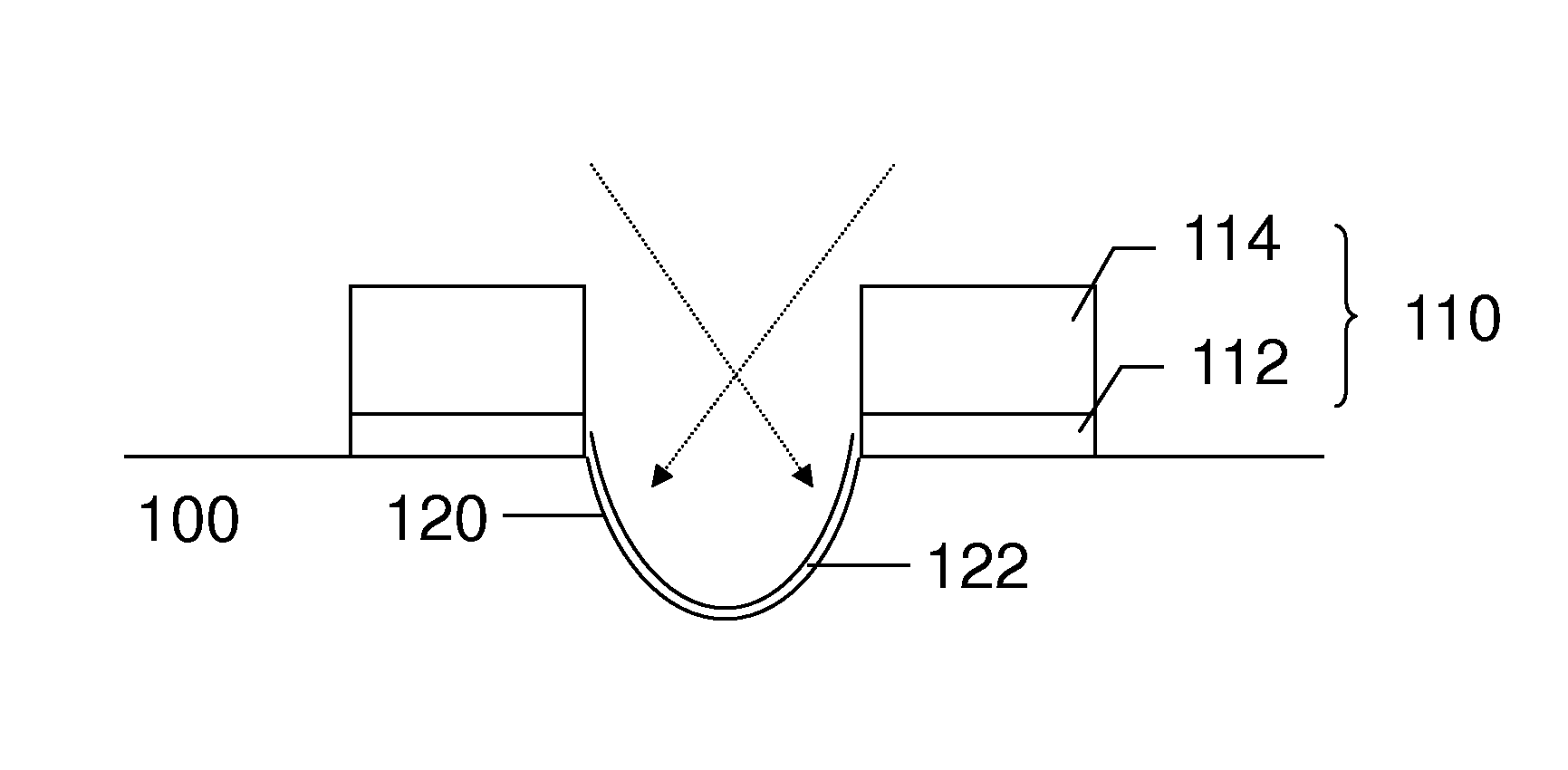
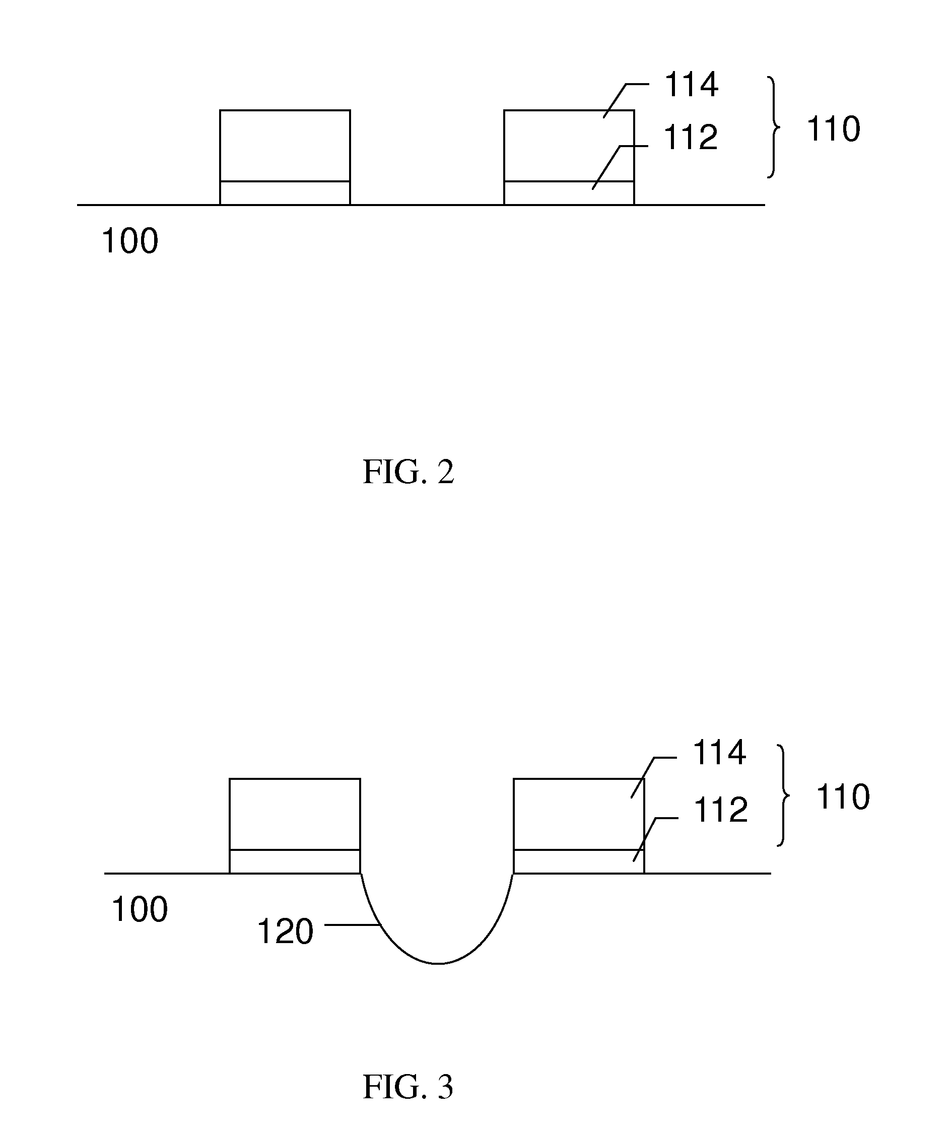
[0015] A fabricating method of the present invention for solving the problems and disadvantages of the prior art is illustrated by an embodiment as follows. Referring to FIG. 2, a patterned mask 110 is located above a silicon substrate 100 of a semiconductor device. The patterned mask 110 illustrated here comprises a sacrificial oxide layer 112 and a silicon nitride layer 114 disposed on the sacrificial oxide layer 112. Such a patterned mask 110 may be formed by sequentially forming a sacrificial oxide layer through a thermal oxidation process and depositing a silicon nitride layer, and then etching the sacrificial oxide layer and the silicon nitride layer with a proper mask.
[0016] Thereafter, with reference to FIG. 3, a recessed trench 120 is formed in the substrate 100 by using the patterned mask110 as a mask. Specifically, an anisotropic etching process, such as RIE (Reactive Ion Etch), or an isotropic etching process is used to etch the substrate 100 to an appropriate depth. Th...
PUM
 Abstract
Description
Claims
Application Information