Multiple output charge-coupled devices

Active Publication Date: 2008-01-24
SEMICON COMPONENTS IND LLC
View PDF21 Cites 6 Cited by
  • Summary
  • Abstract
  • Description
  • Claims
  • Application Information

AI Technical Summary

Benefits of technology

[0013]The present invention has the following advantages of reading out a full resolution image or a reduced resolution higher frame r

Problems solved by technology

They require a striped color filter arrangement that is undesirable for good image quality.
They also do not allow for horizontal summing of pixels for increased frame rate.
This is a more complex HCCD clock driver that requires more components.

Method used


Image

  • Multiple output charge-coupled devices
  • Multiple output charge-coupled devices
  • Multiple output charge-coupled devices

Examples


first embodiment

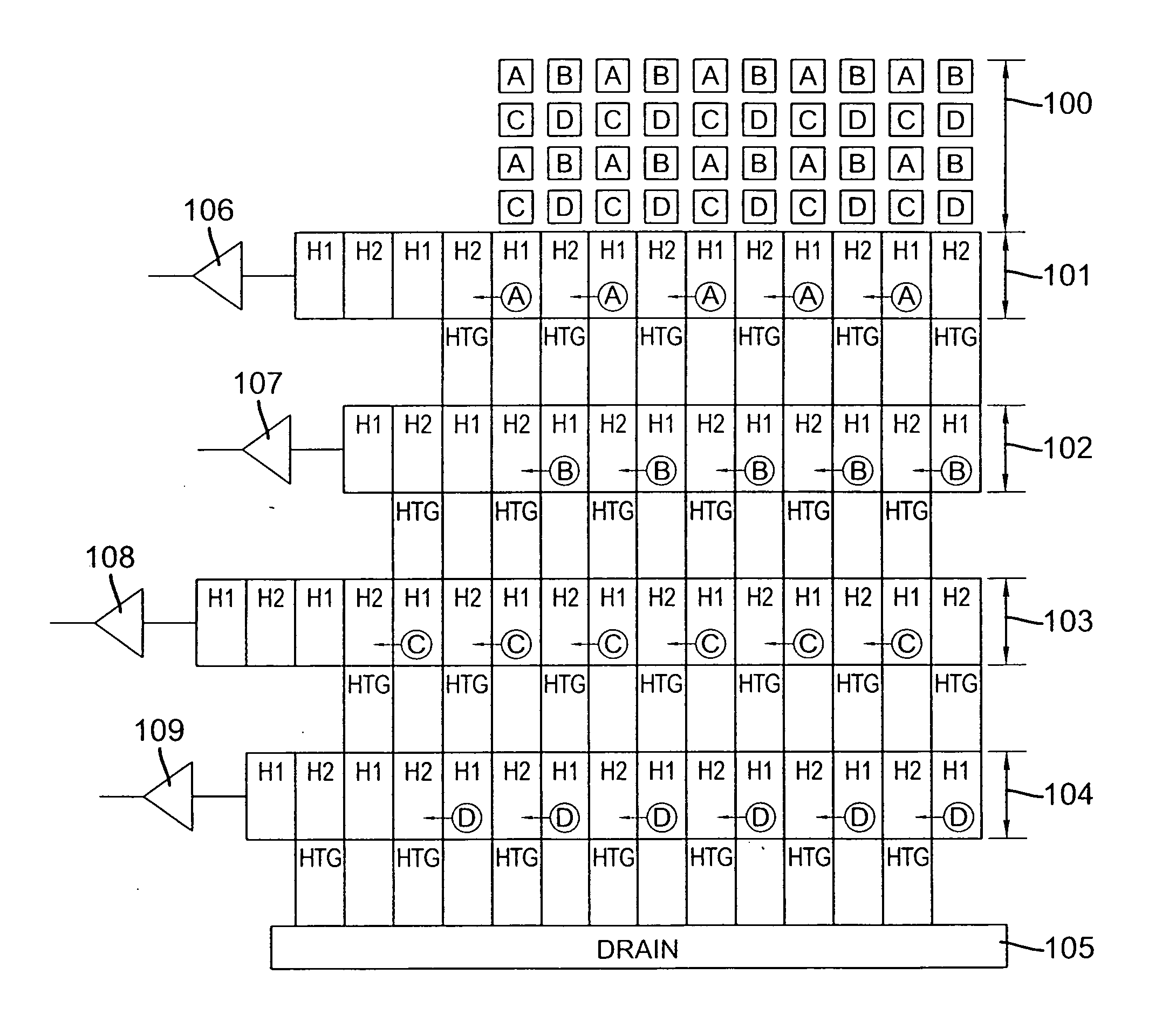
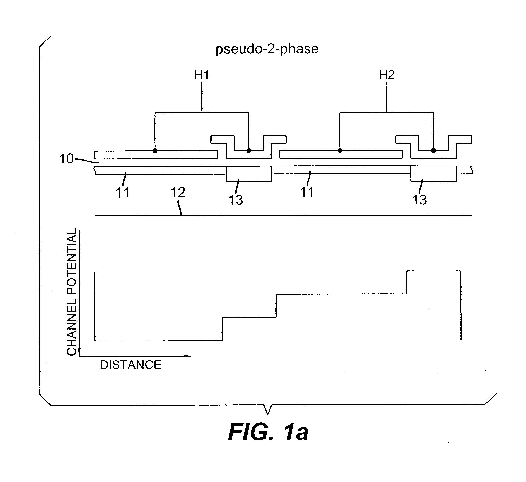
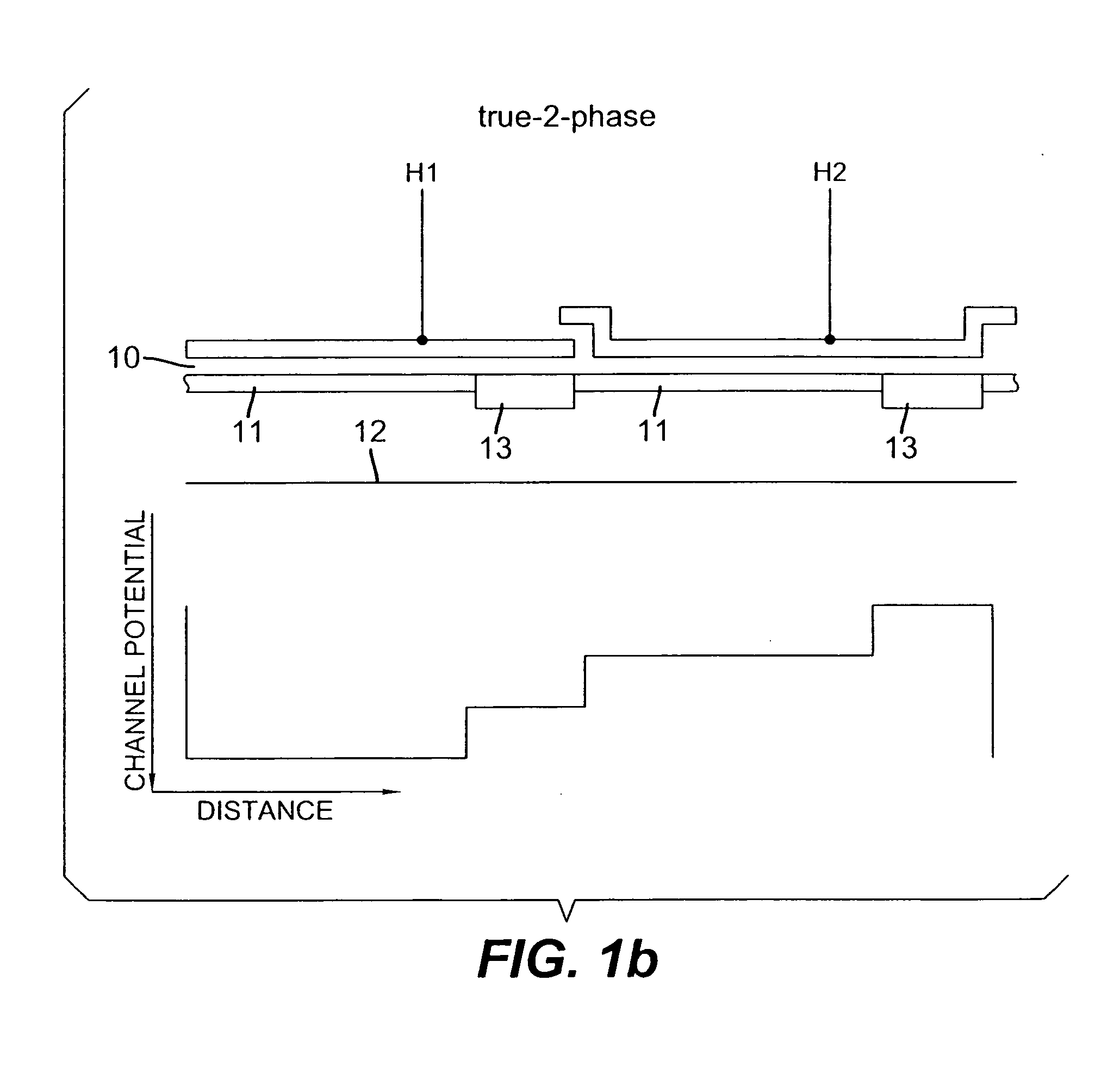
[0054]the present invention is shown in FIG. 2. It is an image sensor with a plurality of pixels 100 of colors A, B, C, and D. The colors are typically, but not limited to, the Bayer color filter pattern where A and D are green, B is blue, and C is red. There are more than two horizontal charge-coupled devices (HCCD) 101, 102, 103, and 104. The present invention is not limited to only four HCCDs, more than four is an extension of the example shown in FIG. 2, as will be apparent to those skilled in the art. Each HCCD is driven by the same two clock signals H1 and H2. The gates H1, and H2 alternate with one gate per column of the pixel array. Each gate H1 or H2 may be a true-2-phase CCD gate or a pseudo-2-phase CCD gate. When the H1 and H2 gates are clocked in a complimentary manner, charge in all of the HCCDs are shifted towards the charge sensing output amplifiers 106, 107, 108, and 109 at the end of each HCCD. Between each HCCD is a transfer gate HTG that allows charge to transfer ...

second embodiment

[0061]The half resolution double speed video readout mode of the second embodiment is now described. The process begins with FIG. 6 where a first row is transferred from the pixel array 200 into the top two HCCDs. Color C enters the 1A and 1B gates of HCCD 201 and color D passes through the 2A and 2B gates of HCCD 201 and into the TG1 gate.

[0062]The next step is shown in FIG. 7. The color charge packet C under the 1B gate in HCCD 201 advances forward two gates while the color charge packet C under the 1A gate remains stationary. This will sum together the two color charge packets C. The same process takes place in HCCD 202 after the color D charge packets are transferred out of the TG1 gate into HCCD 202. FIG. 8 shows the result of the charge summing. The double circle around the charge packets C and D indicates they represent the sum of two charge packets.

[0063]Next, the color D charge packets are transferred under the TG gates in region 221 and held there while the color C charge ...

third embodiment

[0071]the invention shows how three horizontal pixels of the same color may be summed together within the HCCD. This provides for a ⅓rd resolution image readout at video frame rates.

[0072]FIG. 18 shows a third embodiment. It is an image sensor with a plurality of pixels 400 of colors A, B, C, and D. The colors are typically, but not limited to, the Bayer color filter pattern where A and D are green, B is blue, and C is red. It may also be a single color device where A, B, C, and D are all the same color or of no color (pan-chromatic). There are four HCCD shift registers 401, 402, 403, and 404 with charge sensing output amplifiers 408, 409, 410, and 411. The first two HCCD shift registers 401 and 402 have three gates H1, H2, and H3. The H1 and H2 gates alternate with every sixth gate being and H3 gate. All gates labeled H1 are connected together. All gates labeled H2 are connected together. All gates labeled H3 are connected together. The other two HCCD shift registers 403 and 404 in...


PUM


Abstract

An image sensor includes a plurality of pixels overlaid with a color filter pattern of at least two colors having the same color on every other pixel in one direction; three or more charge-coupled devices oriented parallel to the every other pixel color filter repeat pattern; a charge sensing amplifier at the output of at least two of the charge couple devices; each charge-coupled device having a first and a second gate; a CCD-to-CCD transfer gate connecting adjacent charge-coupled devices with the first gate being on one side of the CCD-to-CCD transfer gate and the second gate being on the opposite side of the CCD-to-CCD transfer gate; all CCD-to-CCD transfer gates are electrically connected together; all first gates are electrically connected; and all second gates are electrically connected.

Description

FIELD OF THE INVENTION[0001]The invention relates generally to the field of more than two horizontal charge-coupled devices for reading out an array of pixels, and in particular, for allowing multiple horizontal charge-coupled devices (CCDs) to read out full resolution images or reduced resolution images at video frame rates with pixel summing.BACKGROUND OF THE INVENTION[0002]U.S. Pat. Nos. 4,513,313; 5,164,807; 5,841,554; and US Patent Publication 2005 / 0062868 describe a multiple output horizontal charge-coupled device (HCCD) that distributes m columns of charge to m HCCD registers. Such an output structure does not separate the charge from a Bayer color filter pattern into one color per register. They require a striped color filter arrangement that is undesirable for good image quality. They also do not allow for horizontal summing of pixels for increased frame rate.[0003]The present invention will allow use of the Bayer color filter pattern and will allow for horizontal summing o...

Claims


Application Information

Patent Timeline
IPC IPC(8): H04N5/335
CPCH01L27/14621H01L27/14831H01L27/14887H01L29/768H04N9/045H04N5/3458H04N5/347H04N5/37213H04N5/335H04N25/46H04N25/00H04N25/713H04N25/70H04N25/447H04N25/134
Inventor PARKS, CHRISTOPHER
Owner SEMICON COMPONENTS IND LLC
Why Eureka
Try Eureka