Liquid crystal display device

a liquid crystal display and display technology, applied in semiconductor devices, instruments, optics, etc., can solve the problems of increasing the panel size of the liquid crystal display device, prone to degradation in the quality of display, and becoming eviden

Inactive Publication Date: 2008-01-31
JAPAN DISPLAY INC
View PDF23 Cites 82 Cited by
  • Summary
  • Abstract
  • Description
  • Claims
  • Application Information

AI Technical Summary

Problems solved by technology

Since the common electrode 23 is formed of the transparent electrode such as ITO that has higher sheet resistivity than ordinary metal, the degradation in the quality of display is prone to be caused.
This problem becomes evident particularly as a panel size o

Method used


Image

  • Liquid crystal display device
  • Liquid crystal display device
  • Liquid crystal display device

Examples


first embodiment

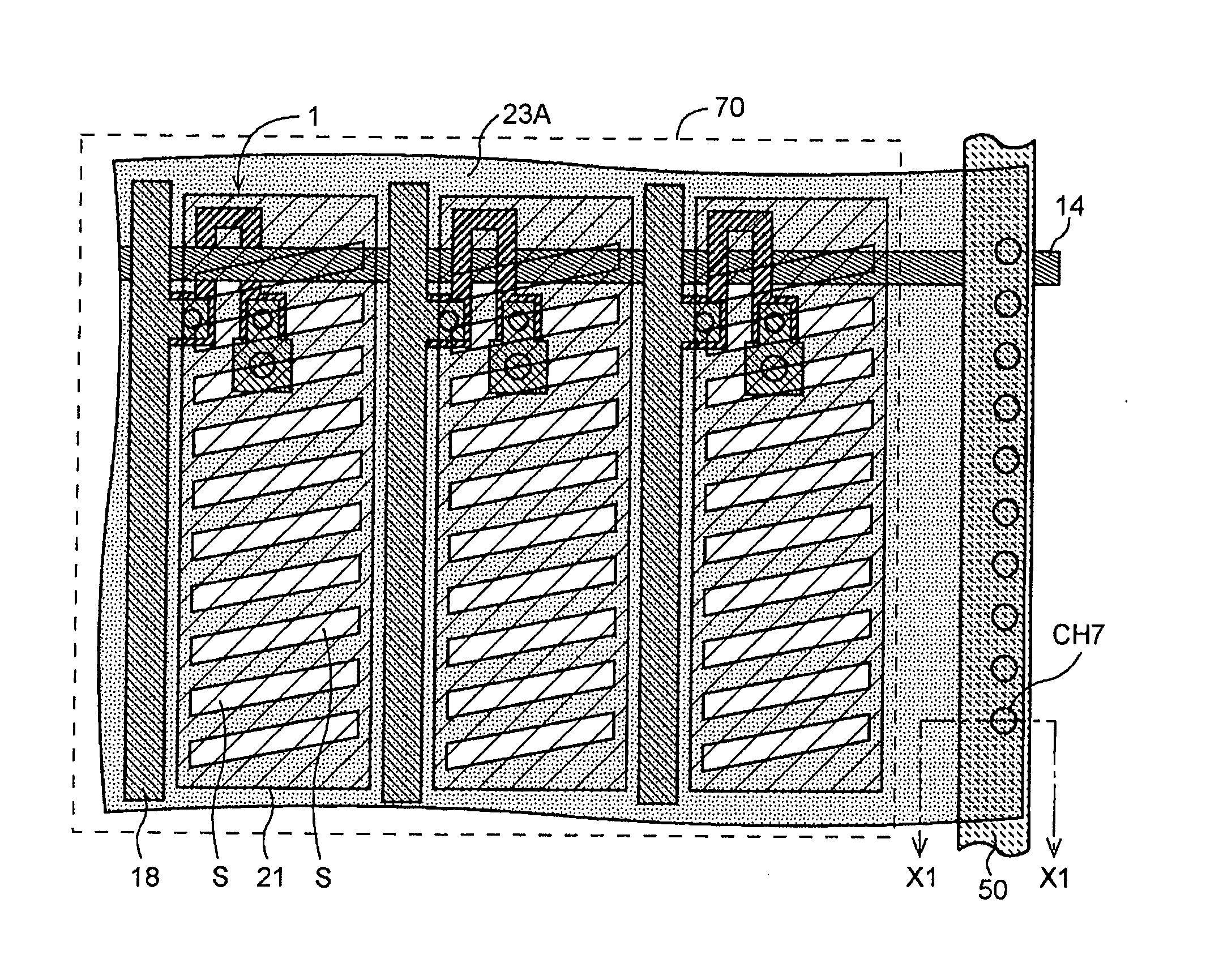
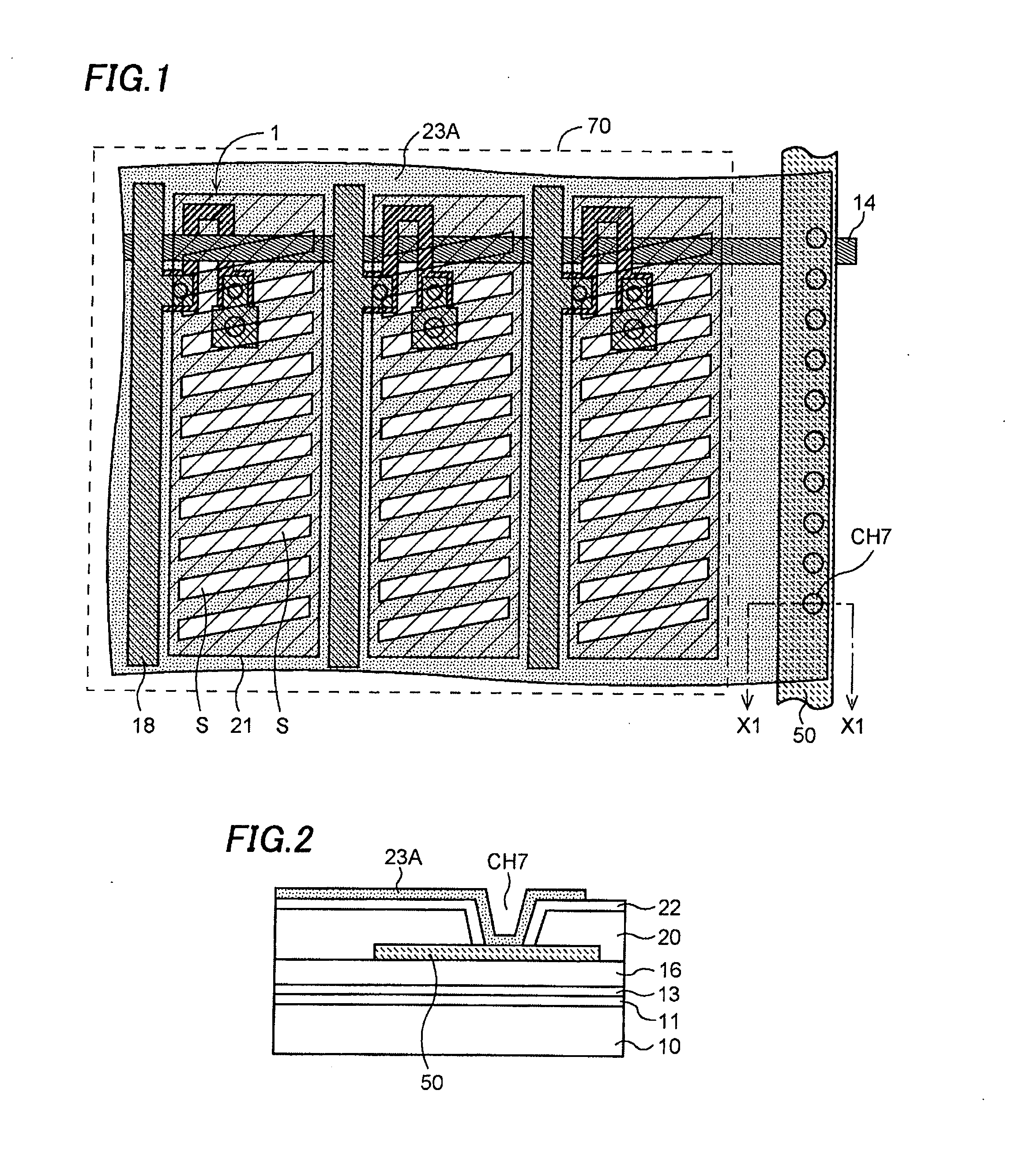
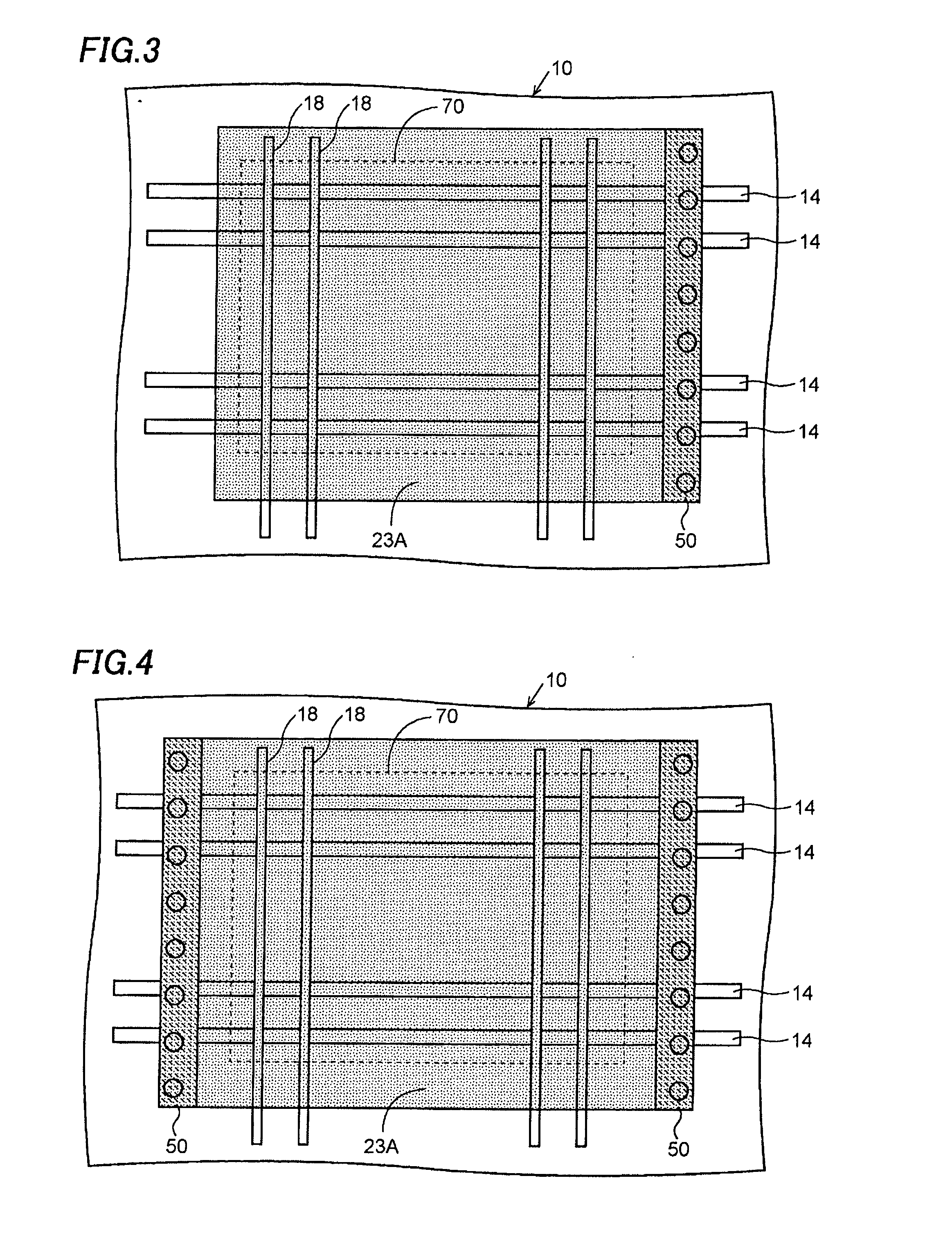
[0039]A liquid crystal display device according to this invention will be explained referring to the drawings. FIG. 1 is a plan view showing a portion of a display region in the liquid crystal display device. FIG. 2 is a cross-sectional view showing a section X1-X1 in FIG. 1. Although a large number of pixels are disposed in a matrix form in the display region 70 in the actual liquid crystal display device, only three pixels are shown in the plan view.

[0040]A pixel electrode 21 is formed of a first layer transparent electrode. A common electrode 23A made of a second layer transparent electrode is formed above the pixel electrode 21 interposing an insulation film 22 between them. The common electrode 23A in an upper layer is provided with a plurality of slits S. The structures described above are generally common to the structure shown in FIGS. 20A and 20B. In the embodiment, however, the common electrode 23A extends over all the pixels in the display region 70. An end of the common ...

second embodiment

[0048]A liquid crystal display device according to this invention will be explained referring to the drawings. FIG. 9 is a plan view showing a portion of a display region in the liquid crystal display device. FIG. 10 is a cross-sectional view showing a section X2-X2 in FIG. 9. FIG. 11 is a cross-sectional view showing a section Y1-Y1 in FIG. 9. Although a large number of pixels are disposed in a matrix form in the display region in the actual liquid crystal display device, only three pixels are shown in the plan view.

[0049]A relationship between vertical locations of the pixel electrode 21 and the common electrode 23A in the liquid crystal display device according to the first embodiment is reversed in the liquid crystal display device according to the second embodiment. A common electrode 23B is formed of the first layer transparent electrode and a pixel electrode 21B is formed of the second layer transparent electrode above it interposing the insulation film 22 between them. The p...

fourth embodiment

[0063]A liquid crystal display device according to this invention will be explained referring to the drawings. FIG. 15 is a plan view showing a portion of a display region in the liquid crystal display device. FIG. 16 is a cross-sectional view showing a section X4-X4 in FIG. 15. FIG. 16 is a cross-sectional view showing a section Y3-Y3 in FIG. 15. Although a large number of pixels are disposed in a matrix form in the display region in the actual liquid crystal display device, only three pixels are shown in the plan view.

[0064]A relationship between vertical locations of the pixel electrode 121B and the common electrode 123B in the liquid crystal display device according to the third embodiment is reversed in the liquid crystal display device according to the fourth embodiment. A pixel electrode 121A is formed of a first layer transparent electrode and a common electrode 123A is formed of a second layer transparent electrode above it interposing a gate insulation film 101 and an inte...


PUM


Abstract

This invention offers a liquid crystal display device according to FFS technology, which is capable of sufficiently providing a common electrode with common electric potential and improving an aperture ratio of pixels to obtain a bright display. A pixel electrode is formed of a first layer transparent electrode. A common electrode made of a second layer transparent electrode is formed above the pixel electrode interposing an insulation film between them. The common electrode in an upper layer is provided with a plurality of slits. The common electrode extends over all the pixels in a display region. An end of the common electrode is disposed on a periphery of the display region and connected with a peripheral common electric potential line that provides a common electric potential Vcom. There is provided neither an auxiliary common electrode line nor a pad electrode, both of which are provided in a liquid crystal display device according to a conventional art.

Description

CROSS-REFERENCE OF THE INVENTION[0001]This application claims priority from Japanese Patent Application No. 2006-204624, the content of which is incorporated herein by reference in its entirety.BACKGROUND OF THE INVENTION[0002]1. Field of the Invention[0003]This invention relates to a liquid crystal display device, specifically to a liquid crystal display device in which an alignment direction of liquid crystal molecules is controlled by a lateral electric field generated between a pixel electrode and a common electrode.[0004]2. Description of the Related Art[0005]As a way to achieve a wide viewing angle of the liquid crystal display device, a method has been developed to realize a light switching function by rotating the liquid crystal molecules in a plane parallel to a substrate with a lateral electric field generated between the electrodes on the same substrate. In-Plane Switching (hereafter referred to as IPS) technology and Fringe-Field Switching (hereafter referred to as FFS) ...

Claims


Application Information

Patent Timeline
IPC IPC(8): G09G3/36G02F1/1343
CPCG02F1/134363G02F2001/134372G02F1/136227G02F1/134372G02F1/1343G02F1/133G02F1/1345G02F1/133357G02F1/136295G02F1/133345G02F1/13439G02F1/136286G02F1/1368G02F2201/40G02F1/134336G02F2202/103G02F2202/104G02F2201/121G02F2201/123H01L27/1222H01L27/1244H01L29/78669H01L29/78678
Inventor ONOGI, TOMOHIDESEGAWA, YASUO
Owner JAPAN DISPLAY INC
Why Eureka
Try Eureka