Liquid crystal display

a technology of liquid crystal display and data driving circuit, which is applied in the direction of static indicating devices, instruments, non-linear optics, etc., can solve the problems of large manufacturing cost, power consumption increase, and difficulty in integrating data driving circuits with display panels, so as to reduce the cost reduce the driving voltage of data driving circuits

Inactive Publication Date: 2008-01-31
SAMSUNG ELECTRONICS CO LTD
View PDF17 Cites 28 Cited by
  • Summary
  • Abstract
  • Description
  • Claims
  • Application Information

AI Technical Summary

Benefits of technology

[0009]Some embodiments of the present invention have been made in an effort to provide a liquid crystal display having advantages of reducing the cost of data driving circuit IC chips and reducing a driving voltage of a data driving circuit. An exemplary embodiment of the present invention provides a liquid crystal display including a substrate, and a plurality of gate lines formed on the substrate, data lines, thin film transistors, pixel electrodes, and storage electrode lines. The gate lines are formed on the substrate. The data lines are arranged crosswise relative to the gate lines, and the thin film transistors are connected to the gate lines and the data lines. The pixel electrodes are connected to the thin film transistors, and each pixel electrode has a first side formed in parallel with the gate lines and a second side shorter than the first side and adjacent to the first side. The storage electrode lines overlap with the pixel electrodes. In the liquid crystal display, a storage electrode signal applied to a storage electrode line is a periodic alternating signal.

Problems solved by technology

Such ICs are responsible for a large share of the manufacturing cost of a liquid crystal display.
However, it is difficult to integrate the data driving circuit with display panel because the data driving circuit has a complicated structure.
The power consumption increases if a driving voltage of the data driving circuit is increased, and the heat generated by the data driving circuit increases as a square of the driving voltage.
The data driving circuit may be damaged by excessive heat.

Method used


Image

  • Liquid crystal display
  • Liquid crystal display
  • Liquid crystal display

Examples


Embodiment Construction

[0040]Below, exemplary embodiments of the present invention are described with reference to the accompanying drawings. As those skilled in the art will realize, these exemplary embodiments may be modified in different ways, all without departing from the spirit or scope of the present invention.

[0041]In the drawings, the thickness of layers, films, panels, regions, etc., is exaggerated for clarity. Like reference numerals designate like elements throughout the specification. It will be understood that when an element such as a layer, a film, a region, or a substrate is referred to as being “on” another element, this can mean “directly on” or intervening elements may be present. In contrast, when an element is referred to as being “directly on” another element, there are no intervening elements present.

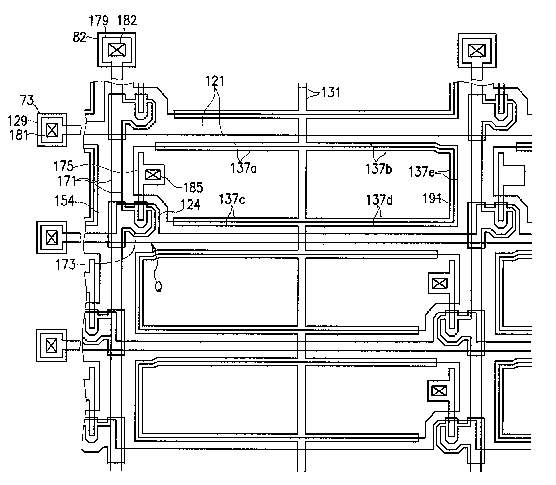
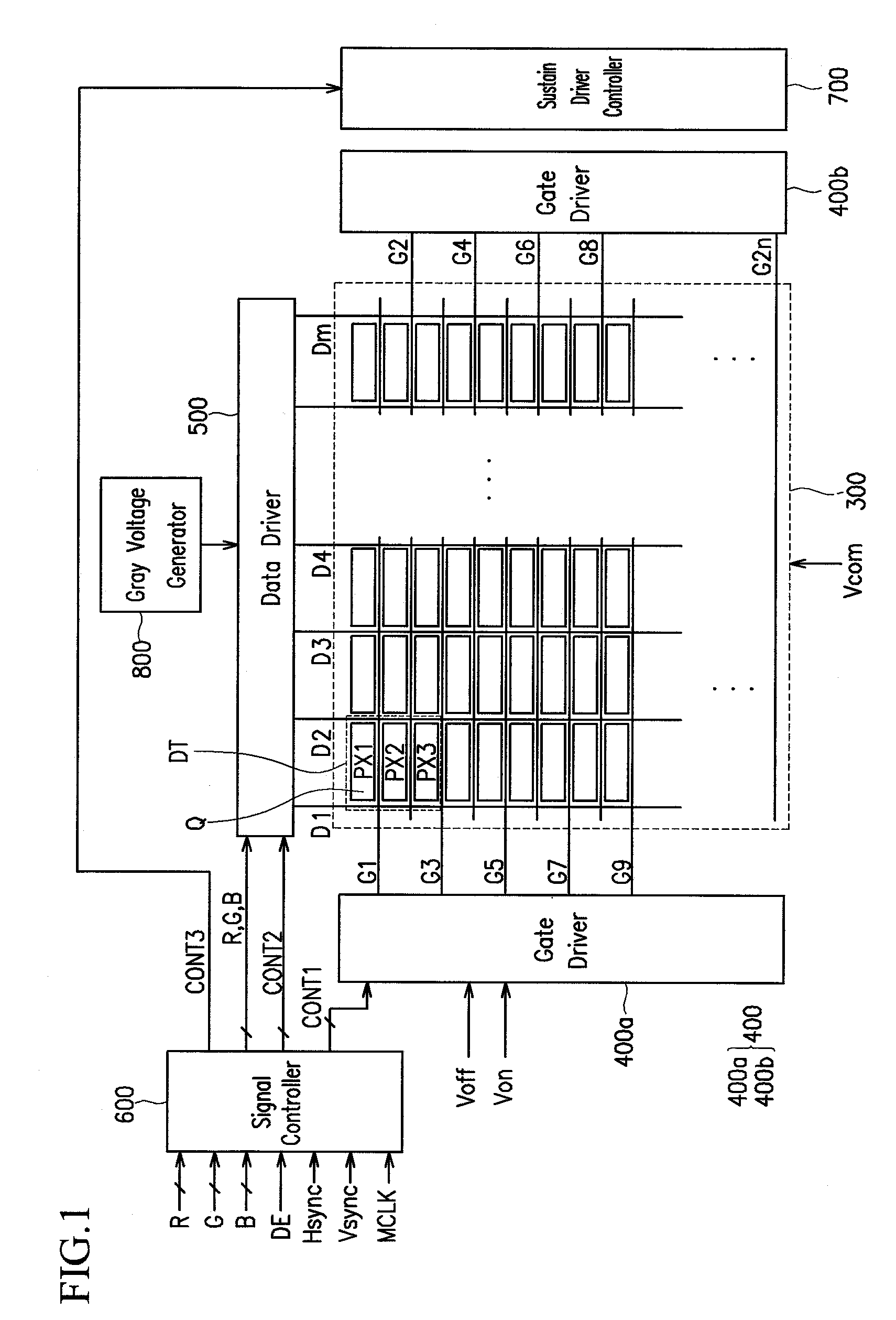
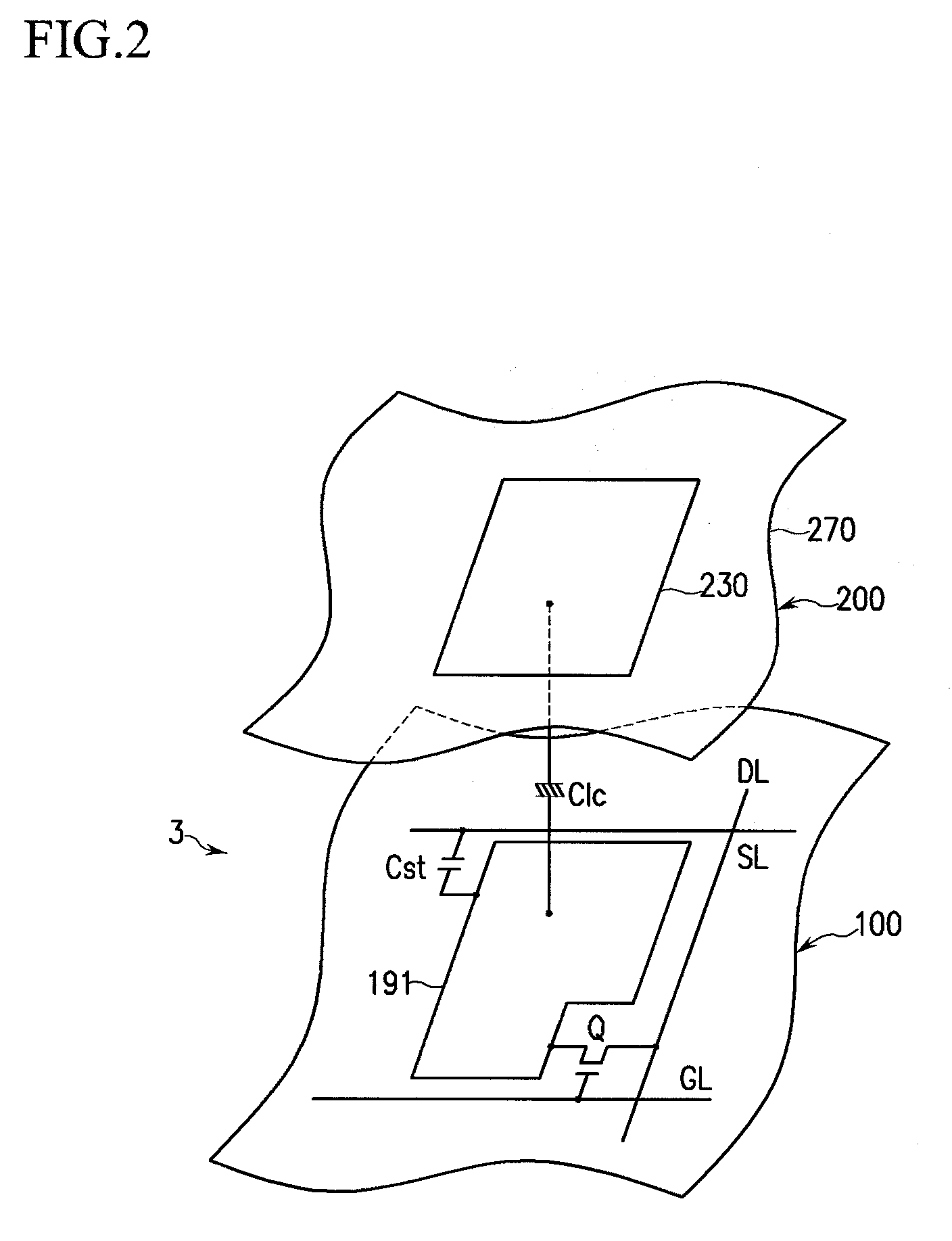
[0042]A liquid crystal display according to one exemplary embodiment of the present invention will now be described with reference to FIG. 1 and FIG. 2. FIG. 1 is a block diagram of th...


PUM

PropertyMeasurementUnit
sidewall angleaaaaaaaaaa
dielectric constantaaaaaaaaaa
polaritiesaaaaaaaaaa

Abstract

A liquid crystal display includes a plurality of pixels arranged in a matrix, a substrate, and a plurality of gate lines, data lines, thin film transistors, pixel electrodes, and storage electrode lines. The gate lines are formed on the substrate. The data lines run crosswise relative to the gate lines above or below the gate lines, and the thin film transistors are connected to the gate lines and the data lines. The pixel electrodes are connected to the thin film transistors, and have a first side formed in parallel with the gate lines and a second side shorter than the first side and adjacent to the first side. The storage electrode lines overlap with the pixel electrodes. Storage electrode signals applied to the storage electrode lines are periodic alternating signals.

Description

CROSS-REFERENCE TO RELATED APPLICATION[0001]This application claims priority to and the benefit of Korean Patent Application No. 10-2006-0069647 filed in the Korean Intellectual Property Office on Jul. 25, 2006, the entire contents of which are incorporated herein by reference.BACKGROUND OF THE INVENTION[0002](a) Field of the Invention[0003]The present invention relates to liquid crystal displays.[0004](b) Description of the Related Art[0005]A liquid crystal display is one of the most widely used types of flat panel displays. A liquid crystal display includes two display panels having field-generating electrodes such as pixel electrodes and a common electrode, and a liquid crystal layer interposed between the panels. The liquid crystal display induces an electric field on a liquid crystal layer by applying voltages to the field generating electrodes. The electric field determines the alignment of liquid crystal molecules in the liquid crystal layer, and this alignment controls the p...

Claims


Application Information

Patent Timeline
Patent Type & Authority Applications(United States)
IPC IPC(8): G02F1/1343
CPCG09G3/3655G09G3/3677G09G3/3688G09G2330/021G09G2300/0426G09G2300/0439G09G2300/0408G02F1/133G02F1/1343
Inventor MOON, SEUNG-HWAN
Owner SAMSUNG ELECTRONICS CO LTD
Why Eureka
Try Eureka