Method for reading a multi-level passive element memory cell array

a memory cell array and multi-level technology, applied in static storage, digital storage, instruments, etc., can solve the problems of performance penalties and likely three long read cycles, and achieve the effect of decreasing resistance levels, decreasing resistance levels, and decreasing resistance levels

Active Publication Date: 2008-01-31
SANDISK TECH LLC
View PDF51 Cites 181 Cited by
  • Summary
  • Abstract
  • Description
  • Claims
  • Application Information

AI Technical Summary

Benefits of technology

[0012]In one aspect, the invention provides a method for reading a multi-level passive element memory cell having first, second, third, and fourth memory cell states corresponding respectively to first, second, third, and fourth decreasing resistance levels. The method includes discriminating between memory cell states by sensing current on a selected bit line for at least two different combinations of reference current level and read bias voltage on the selected bit line.
[0013]In another aspect, the invention provides a method for reading a multi-level passive element memory cell having first, second, third, and fourth memory cell states corresponding respectively to first, second, third, and fourth decreasing resistance levels. The method includes biasing a selected bit line with a read bias voltage, biasing a selected word line with a selected word line voltage, generating a first signal and a second signal indicative respectively of a current on the selected bit line relative to a first reference current level and relative to a second reference current level, and generating a read data value for a first data bit as a function of the first and second signals.
[0014]In another aspect, the invention provides a method for reading a multi-level passive element memory cell having first, second, third, and fourth memory cell states corre

Problems solved by technology

Writing and reading memory cells with more than two levels stored in each cell leads to performance penalties because multiple write cycles and multiple read cycles are required.
In 3D passive element arrays this is a particular problem because of the othe

Method used


Image

  • Method for reading a multi-level passive element memory cell array
  • Method for reading a multi-level passive element memory cell array
  • Method for reading a multi-level passive element memory cell array

Examples


Embodiment Construction

)

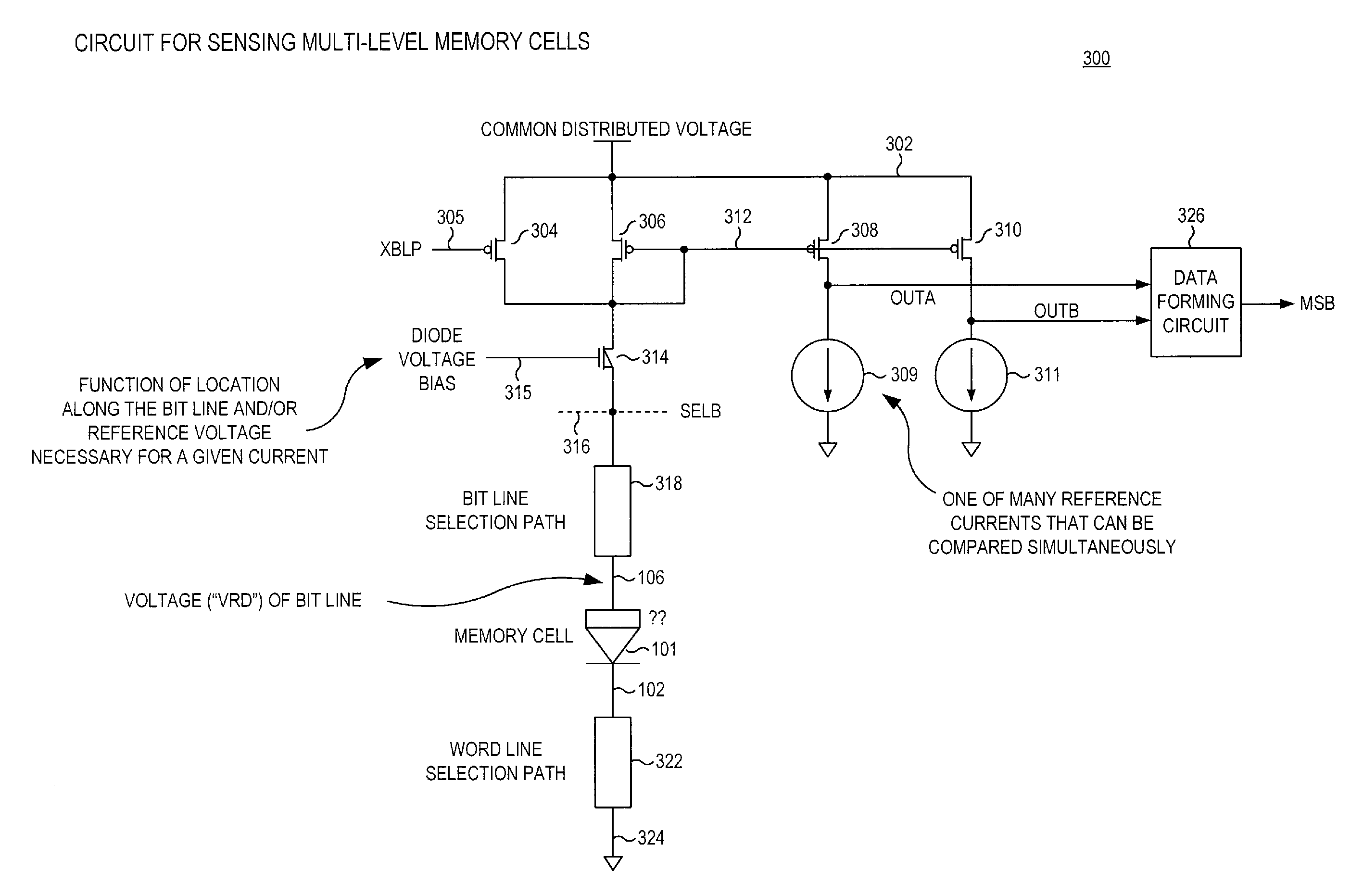
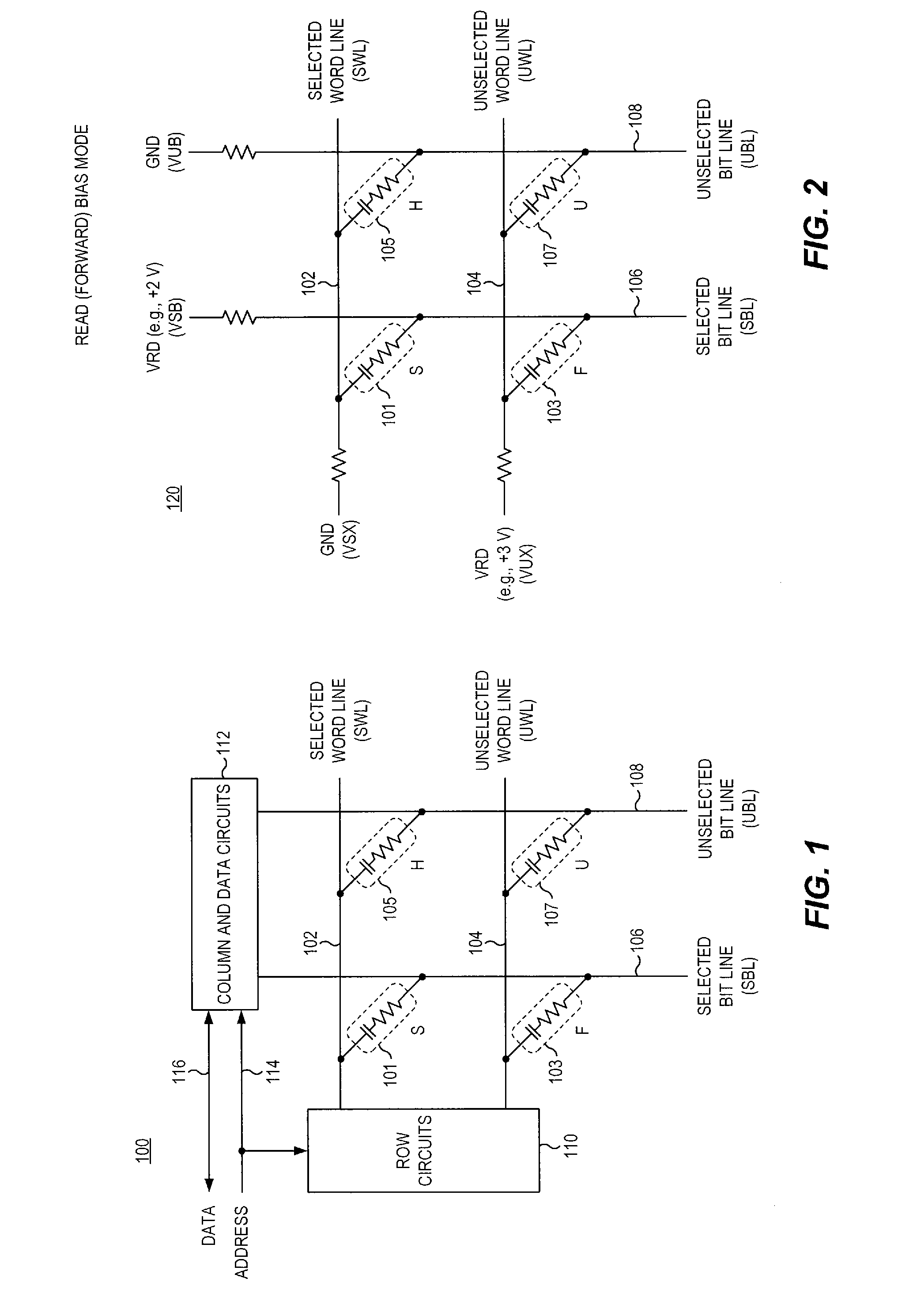
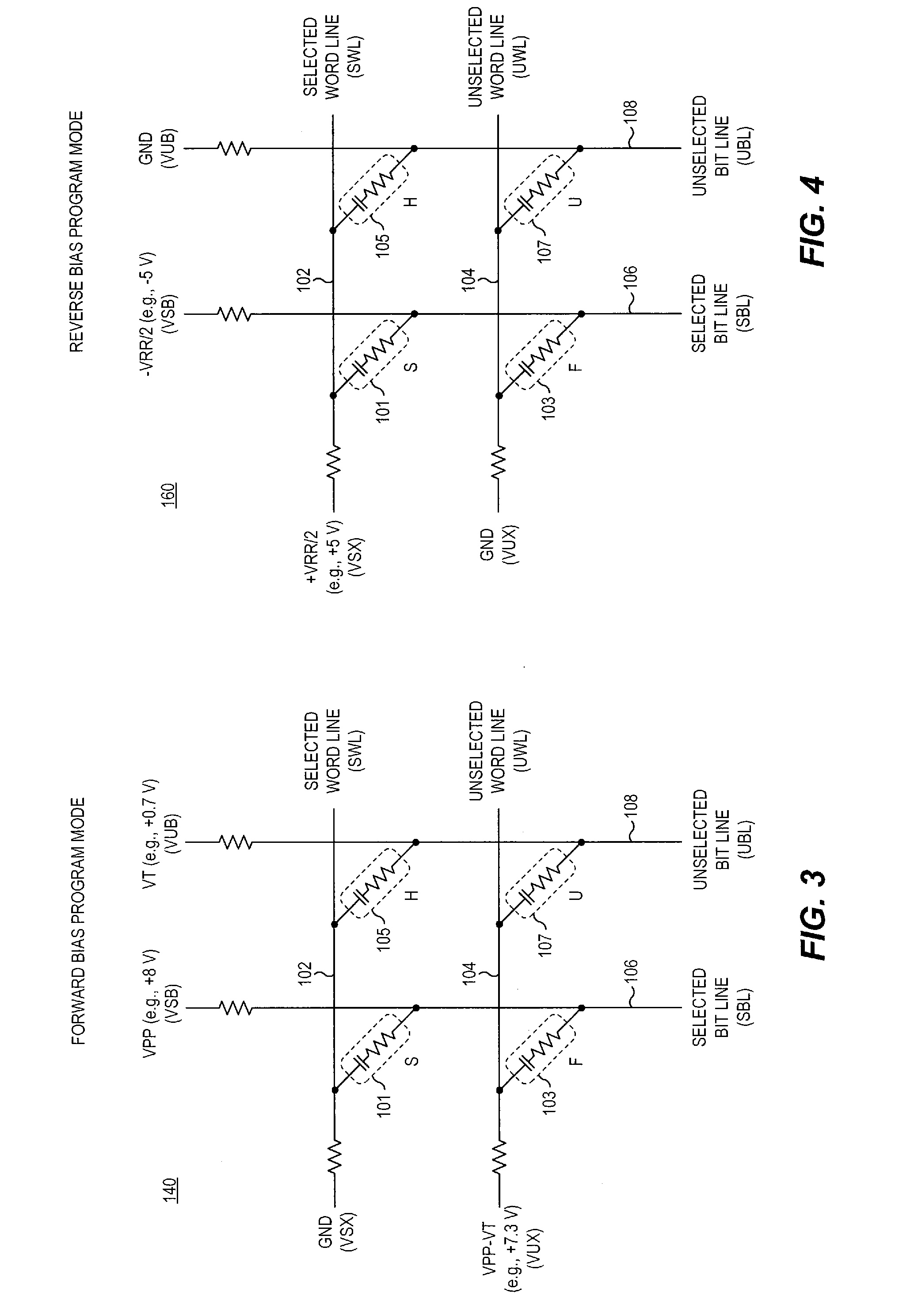
[0030]FIG. 1 is a schematic diagram of an exemplary passive element memory array 100. Two word lines 102, 104 are shown, as well as two bit lines 106, 108. Word line 102 is assumed to be a selected word line (SWL), and word line 104 is assumed to be an unselected word line (UWL). Similarly, bit line 106 is assumed to be a selected bit line (SBL), and bit line 108 is assumed to be an unselected bit line (UBL). Four passive element memory cells 101, 103, 105, 107 are shown, each coupled between an associated word line and an associated bit line.

[0031]Memory cell 101 is associated with the selected word line 102 and the selected bit line 106, and may be viewed as an “S” cell (i.e., “selected” cell). Memory cell 103 is associated with the unselected word line 104 and the selected bit line 106, and may be viewed as an “F” cell (i.e., “off” cell). Memory cell 105 is associated with the selected word line 102 and the unselected bit line 108, and may be viewed as an “H” cell (i.e., “half-s...


PUM


Abstract

A four level passive element cell has memory states corresponding to decreasing resistance levels, which are preferably mapped respectively to data states 11, 01, 00, and 10. The LSB and MSB are preferably mapped as part of different pages. To discriminate between memory cell states, the selected bit line current is sensed for at least two different combinations of reference current level and read bias voltage. A mid-level reference is used to read the LSB. When reading the MSB, a first reference between the 10 and 00 data states, and a second reference between 01 and 11 data states may be used, and the mid-level reference need not be used. In certain embodiments, the bit line current may be simultaneously compared against the first and second references, without requiring a delay to stabilize the bit line current to a different value, and the MSB generated accordingly.

Description

CROSS-REFERENCE TO RELATED APPLICATION(S)[0001]This application discloses subject matter that is also disclosed in the following co-pending U.S. patent application(s), each filed on even date herewith, and each of which is hereby incorporated by reference in its entirety:[0002]U.S. application Ser. No. ______ (Attorney Docket No. 023-0049) entitled “Apparatus for Reading a Multi-Level Passive Element Memory Cell Array” by Roy E. Scheuerlein, Tyler J. Thorp, and Luca G. Fasoli.BACKGROUND[0003]1. Field of the Invention[0004]The present invention relates to semiconductor integrated circuits containing programmable multi-level memory cell arrays, and particularly those arrays incorporating passive element memory cells, and more particularly those having a three-dimensional memory array.[0005]2. Description of the Related Art[0006]Writing and reading memory cells with more than two levels stored in each cell leads to performance penalties because multiple write cycles and multiple read c...

Claims


Application Information

Patent Timeline
IPC IPC(8): G11C16/04
CPCG11C2213/72G11C11/565G11C11/5685G11C11/5692G11C13/0007G11C2213/32G11C17/16G11C17/18G11C2013/0054G11C2211/5631G11C2211/5634G11C13/004
Inventor SCHEUERLEIN, ROY E.THORP, TYLER J.FASOLI, LUCA G.
Owner SANDISK TECH LLC
Why Eureka
Try Eureka