
Semiconductor memory, controller, and operating method of semiconductor memory

a technology of semiconductor memory and memory controller, which is applied in the field of semiconductor memory, can solve the problems the size of the lsi chip, and achieve the effect of increasing the cost of the chip

Inactive Publication Date: 2008-01-31
SOCIONEXT INC
View PDF8 Cites 17 Cited by
  • Summary
  • Abstract
  • Description
  • Claims
  • Application Information

AI Technical Summary

Benefits of technology

[0008]An object of the present invention is to perform mask control of data without increasing the number of external terminals even when the number of bits of a data mask signal is large.
[0009]In the present invention, an address input circuit sequentially receives a first address signal, a second address signal, and a first data mask signal supplied to an address terminal in synchronization with transition edges of a clock signal. That is, the first data mask signal is supplied to the address terminal at a different timing from that at which the first address signal or second address signal is received. The first address signal, second address signal, and first data mask signal are output, for example, from a controller accessing semiconductor memory. A data input / output circuit inputs / outputs data via data terminals. The data input / output circuit masks at least either of write data to memory cells and read data from memory cells in accordance with logic of the first data mask signal. This makes it possible to perform mask control of data without increasing the number of external terminals even when the number of bits in the first data mask signal is large.

Problems solved by technology

Thus, when the number of external terminals increases, chip size of LSI tends to become larger and chip cost tends to become higher.
No technology has been proposed that can mask data without increasing the number of external terminals when the number of bytes of data increases and the number of bits of a data mask signal increases.

Method used


Image

  • Semiconductor memory, controller, and operating method of semiconductor memory
  • Semiconductor memory, controller, and operating method of semiconductor memory
  • Semiconductor memory, controller, and operating method of semiconductor memory

Examples


first embodiment

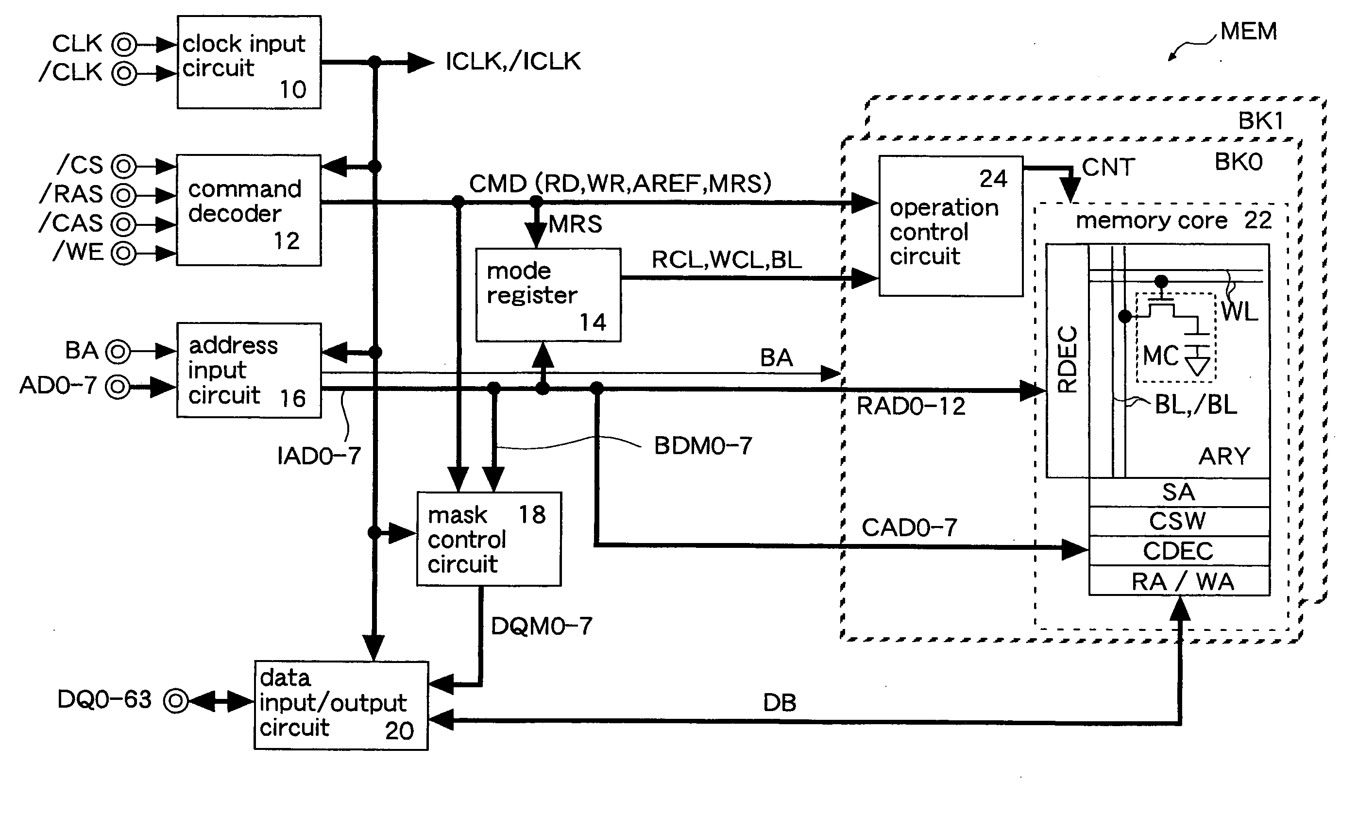
[0026]FIG. 1 shows the present invention. A semiconductor memory MEM is, for example, a clock synchronous type FCRAM (Fast Cycle RAM) operating in synchronization with an external clock CLK. The FCRAM is a pseudo SRAM having memory cells of DRAM and an interface of SDRAM. The memory MEM includes a clock input circuit 10, a command decoder 12, a mode register 14, an address input circuit 16, a mask control circuit 18, a data input / output circuit 20, and banks BK0 and BK1. Each of the banks BK0 and BK1 has a memory core 22 and an operation control circuit 24, and operates independently of each other.

[0027]The clock input circuit 10 receives complementary clock signals CLK and / CLK via clock terminals and supplies the received clocks CLK and / CLK to each circuit block as its internal clocks ICLK and / ICLK. Incidentally, a clock enable signal CKE may be supplied to the clock input circuit 10 to stop generation of the internal clocks ICLK and / ICLK while the clock enable signal CKE is at...

third embodiment

[0064]FIG. 8 shows operations of the A detailed description of the same operation as that described in FIG. 4 is omitted. In this embodiment, when performing a read operation, the data mask signal DM is supplied to the memory MEM each in synchronization with the falling edge and rising edge of the next clock signal CLK after receiving the read command RD. When performing a write operation, the data mask signal DM is supplied to the memory MEM each in synchronization with a supply timing of write data. In this example, as many data mask signals DM as (“4” in this example) corresponding to a burst length are supplied in response to one read command RD or one write command WR.

[0065]Operations up to the third clock cycle are the same as those in FIG. 4. In the read operation, the data mask signals DM of a low logical level L, high logical level H, high logical level H, and low logical level L are supplied one clock before outputting read data D10-17, D20-27, D30-37, and D40-47 respecti...


PUM


Abstract

To perform mask control of data signals without increasing the number of external terminals even when the number of bits in a data mask signal is large, an address input circuit sequentially receives a first address signal, a second address signal, and a first data mask signal supplied to an address terminal in synchronization with transition edges of a clock signal. Namely, the first data mask signal is supplied to the address terminal at a different timing from timing at which the first and second address signals are received. The first address signal, second address signal, and first data mask signal are output, for example, from a controller accessing a semiconductor memory. A data input / output circuit inputs / outputs data via a data terminal and masks at least either of write data to memory cells and read data from the memory cells in accordance with logic of the first data mask signal.

Description

CROSS REFERENCE TO RELATED APPLICATION[0001]This application is based upon and claims the benefit of priority from Japanese Patent Application No. 2006-191685, filed on Jul. 12, 2006, the entire contents of which are incorporated herein by reference.BACKGROUND OF THE INVENTION[0002]1. Field of the Invention[0003]The present invention relates to a semiconductor memory and a controller for accessing the semiconductor memory.[0004]2. Description of the Related Art[0005]With progress of semiconductor manufacturing technology, the number of elements that can be mounted in a controller of an ASIC (Application Specific IC) or the like is increasing year by year. In response to the rising number of elements, it becomes possible to mount various functional blocks chip, which have conventionally been configured by separate chips, on a single ASIC. As ASICs have more advanced features, the number of external terminals tends to increase. Also, in order to increase a data transfer rate, the numb...

Claims


Application Information

Patent Timeline
Patent Type & Authority Applications(United States)
IPC IPC(8): G11C8/18G11C8/00
CPCG11C7/1006G11C7/1045G11C7/1051G11C7/1066G11C7/1078G11C11/4096G11C7/12G11C7/22G11C11/4076G11C11/4094G11C7/1093G11C11/4093G11C11/408
Inventor KANDA, TATSUYASATO, KOTOKU
Owner SOCIONEXT INC
Learn More