Light emitting diode package with positioning groove

a technology of light-emitting diodes and package structures, which is applied in the direction of basic electric elements, electrical apparatus, semiconductor devices, etc., can solve the problems of difficult gel positioning, difficult to distribute fluorescent materials uniformly, and small size of light-emitting diodes, so as to improve gel positioning and solve the problem of overflow

Inactive Publication Date: 2008-02-07
LUSTROUS TECH
View PDF4 Cites 117 Cited by
  • Summary
  • Abstract
  • Description
  • Claims
  • Application Information

AI Technical Summary

Benefits of technology

[0011]An objective of the present invention is to provide a light emitting diode package structure with a groove. When the gel is dispensed, the overflow problem is improved. And the positioning of the gel is improved as well.

Problems solved by technology

Also, light emitting diodes are very small and light.
As a result, it is difficult to position the gel 29 on the light emitting diode 21 precisely.
Moreover, as to the fluorescent materials, it is difficult to distribute the fluorescent materials uniformly in the gel 29.
As a result, some light is wasted.
Furthermore, because the distribution of the fluorescent materials in the gel 29 is not uniform, the light generated by the light emitting diode package structure 20 is not uniform.

Method used


Image

  • Light emitting diode package with positioning groove
  • Light emitting diode package with positioning groove
  • Light emitting diode package with positioning groove

Examples


first embodiment

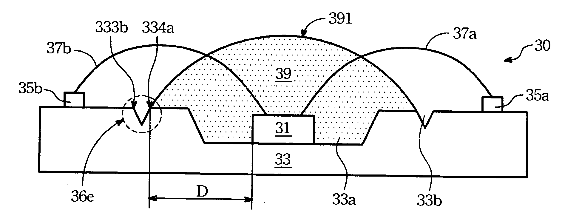
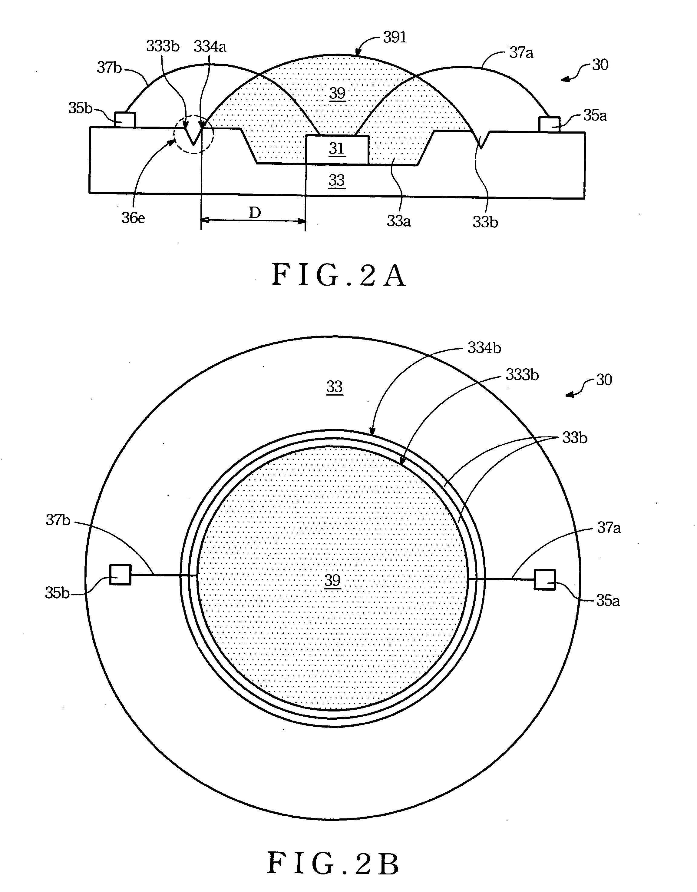
[0029]Please refer to FIG. 2A. FIG. 2A is a sectional side view of a light emitting diode package structure 30 according to the present invention. The light emitting diode package structure 30 includes a light emitting diode 31, a substrate structure 33, electrodes 35a and 35b, wires 37a and 37b, and at least one gel 39. The light emitting diode 31 is the main light emitting component in the light emitting diode package structure 30. The light emitting diode 31 can be a chip. A surface of the substrate structure 33 has a concave 33a and at least one groove 33b. The concave 33a is used for containing the light emitting diode 31. In the present embodiment of the invention, a sectional side view of the groove 33b is a V-shape. The light emitting diode 31 is electrically connected to the electrodes 35a and 35b through the wires 37a and 37b respectively. The gel 39 is transparent, for covering the light emitting diode 31, a portion of the surface of the substrate structure 33, and a port...

second embodiment

[0039]Please refer to FIG. 3A. FIG. 3A is a sectional side view of a light emitting diode package structure 40, according to the present invention. The diode package structure 40 includes a light emitting diode 41, a substrate structure 43, electrodes 45a and 45b, an electrically conductive layer 47, and a gel 49. A surface of the substrate structure 43 has a concave 43a and at least one groove 43b. The groove 43b includes the first groove 43b. The first groove 43b is disposed in the concave 43a. The electrically conductive layer 47 is disposed on the surface of the substrate structure 43. The concave 43a is used for containing the light emitting diode 41. A first predetermined distance (D1) is between the first concave 43b and the light emitting diode 41. The first groove 43b is formed around the light emitting diode 41. The light emitting diode 41 is electrically connected to the electrodes 45a and 45b respectively by the electrically conductive layer 47. At least one gel 49 inclu...

fourth embodiment

[0043]Please refer to FIG. 3C. FIG. 3C is a sectional side view of a light emitting diode package structure 40 according to the present invention. In the present embodiment, functions of most components are similar to or the same as those in the embodiment in FIG. 3B. The difference between the FIG. 3B and FIG. 3C is that the substrate structure 43 in FIG. 3C includes a substrate 431 and a silicon carrier 432. The silicon carrier 432 is disposed in the concave 43a, for containing the light emitting diode 41. The silicon carrier 432 can be manufactured by a micro-electro-mechanical process. The first groove 43b is disposed on a surface of the silicon carrier 432. The first predetermined distance (D1) is between the first groove 43b and the light emitting diode 41. The region covered by the electrically conductive layer 47 does not include the first groove 43b as shown in FIG. 3B. The light emitting diode 41 is disposed on the silicon carrier 432. The silicon carrier 432 electrically ...


PUM


Abstract

A light emitting diode package structure includes a light emitting diode, a substrate structure and at least one gel. A surface of the substrate structure has a concave and at least one groove. The concave is used for containing the light emitting diode. A predetermined distance (D) is between the groove and the light emitting diode. The groove is formed around the light emitting diode. The gel covers the light emitting diode and a portion of the surface of the substrate structure. The gel is limited to surface tension in the groove and is positioned in a predetermined region surrounded by the groove.

Description

BACKGROUND OF THE INVENTION[0001](1) Field of the Invention[0002]The present invention generally relates to a light emitting diode package structure, and particularly to a light emitting diode package structure having a groove to improve the positioning of the gel.[0003](2) Description of the Prior Art[0004]The energy that light emitting diodes (LED) need is much less than the energy that the conventional incandescent lights or fluorescent lights need. Therefore, light emitting diodes are applied to many kinds of electronic products and industries more and more commonly. Also, light emitting diodes are very small and light. Thus, light emitting diodes are much better than conventional light sources. With the trend of electronic products becoming lighter and smaller, the demand of light emitting diodes is increasing day by day.[0005]Please refer to FIG. 1A. FIG. 1A is a sectional side view of a conventional light emitting diode package structure 10. The conventional light emitting di...

Claims


Application Information

Patent Timeline
Patent Type & Authority Applications(United States)
IPC IPC(8): H01L29/227
CPCH01L33/486H01L33/52H01L33/54H01L2224/8592H01L2224/48091H01L2924/00014
Inventor LIU, CHIA-CHICHI, PAO-CHICHANG, YUEH-HISIN
Owner LUSTROUS TECH
Why Eureka
Try Eureka