

Cells of a customizable logic array device having independently accessible circuit elements
a logic array and circuit element technology, applied in the field of customizable logic array devices having independently accessible circuit elements, can solve the problems waste, and the expense of a decrease in active circuit density, and achieve the effect of reducing the number of unused circuit elements and facilitating the use of each of the circuit elements
- Summary
- Abstract
- Description
- Claims
- Application Information
AI Technical Summary
Benefits of technology
Problems solved by technology
Method used
Image

Examples
Embodiment Construction
OF EMBODIMENTS
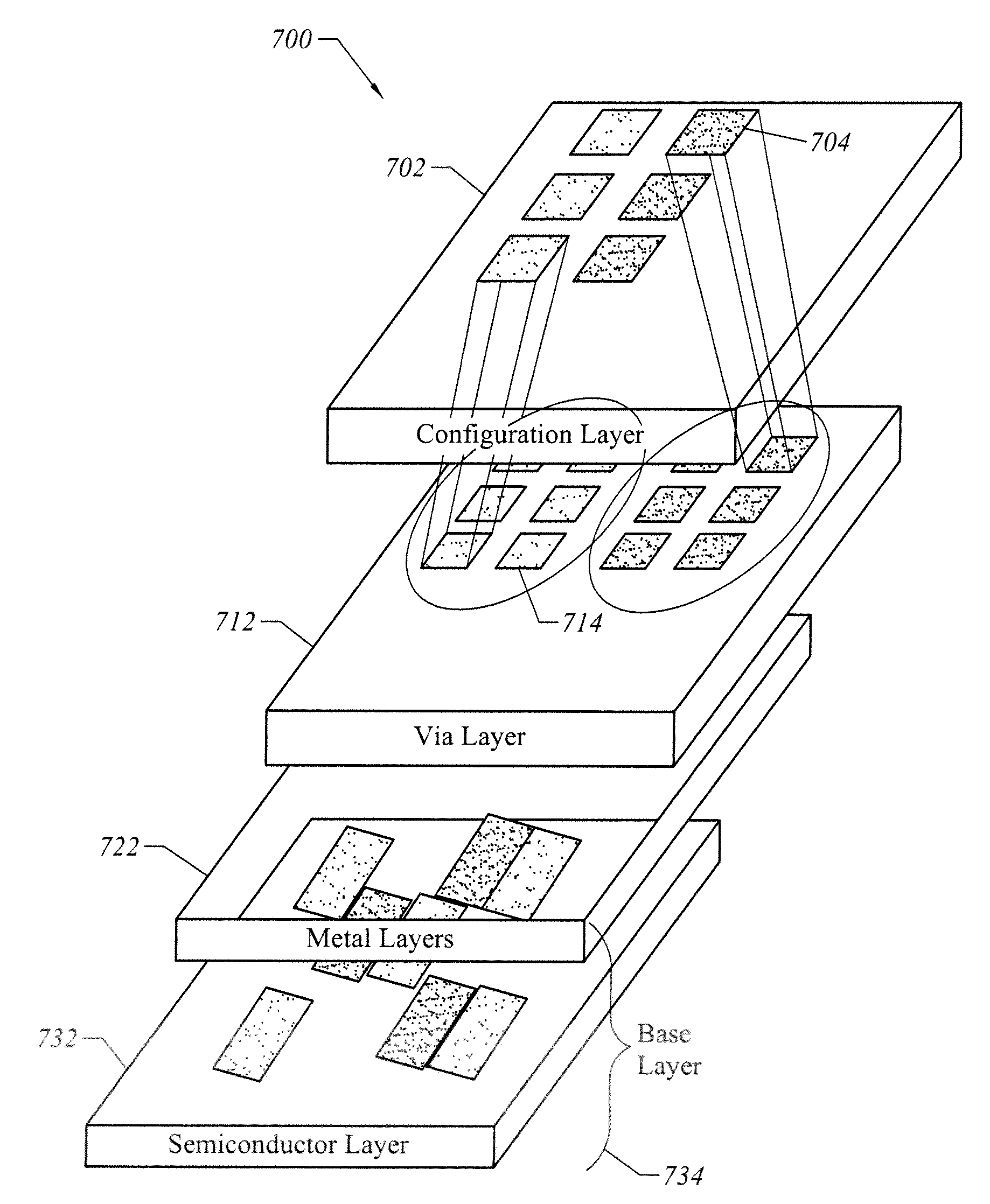
[0025]FIG. 2A is a block diagram illustrating a cell structure for a customizable logic array device, according to at least one specific embodiment of the invention. Cell 200 includes a number of circuit elements 210, 212, 214, and 216, each of which is independently accessible from locations external from cell 200. Circuit elements 210, 212, 214, and 216 include one or more inputs (“I / P”) 202 and one or more outputs (“O / P”) 204 that extend up through an interlayer connection layer, such as via layer 222, to at least to a top layer, such a configuration layer 220. Generally, the interlayer connection layer connects each input 202 and output 204 to configuration layer 220 so as to enable each of the circuit elements to be independently accessible. As used herein, the term “independently accessible” refers in some embodiments to the availability of individual inputs 202 and outputs 204 for either routing with other inputs 202 and outputs 204 of the same or different circ...
PUM
 Abstract
Description
Claims
Application Information