Daisy chainable memory chip

a memory chip and daisy chain technology, applied in the field of memory system and memory interconnection, can solve the problems of buffer chips, memory system cost, buffer chips, etc., and achieve the effect of increasing the cost of buffer chips and memory system

Active Publication Date: 2008-02-07
GLOBALFOUNDRIES US INC
View PDF8 Cites 7 Cited by
  • Summary
  • Abstract
  • Description
  • Claims
  • Application Information

AI Technical Summary

Problems solved by technology

However, L1 caches, while very fast, are also quite small, perhaps 64 KB (Kilobytes) to 256 KB.
A problem with this approach is that buffer chips are required.
Buffer chips also add cost to a memory system.
Yet another problem in this implementation is that a first period of time (one or more cycles) is used to drive the address and command to a buffer chip and a second period of time (one or more cycles) is then used to drive the address on a carrier (e.g., carrier 16).
Ensuring that the chip-module-carrier-module-chip path is operational, and providing for diagnosis of faulty signaling paths, also often requires that some or all pins be driven by a common I / O circuit that can both drive and receive, thus increasing the size and complexity of the circuitry that drives (or receives).

Method used


Image

  • Daisy chainable memory chip
  • Daisy chainable memory chip
  • Daisy chainable memory chip

Examples


second embodiment

[0136]Data words 130 (data words shown in FIGS. 7B and 7C) are driven onto data bus 59A at data bus port 32 (one shown referenced in FIG. 8) by memory controller 52 for writing into a memory chip 54. Data words 130 having data 131 read from a memory chip 54 are received by memory controller 52 on data bus 59N. For example, memory controller 52 needs to write data into memory chip 54A and read data from memory chip 54B. An address / command word 120 is transmitted at address / command bus port 31 (one shown referenced in FIG. 8) on address / command bus 58A and is recognized by memory chip 54A as a write into its array 55 for data having a packet ID value matching the value in packet ID 123 of the address / command word 120. As described earlier, data 131 from a write data word 130 having a packet ID 132 matching the packet ID 123 of address / command word 120 is written into the array 55 of memory chip 54A. The address / command word 120 for the write into memory chip 54A, in an embodiment, is ...

embodiment 700

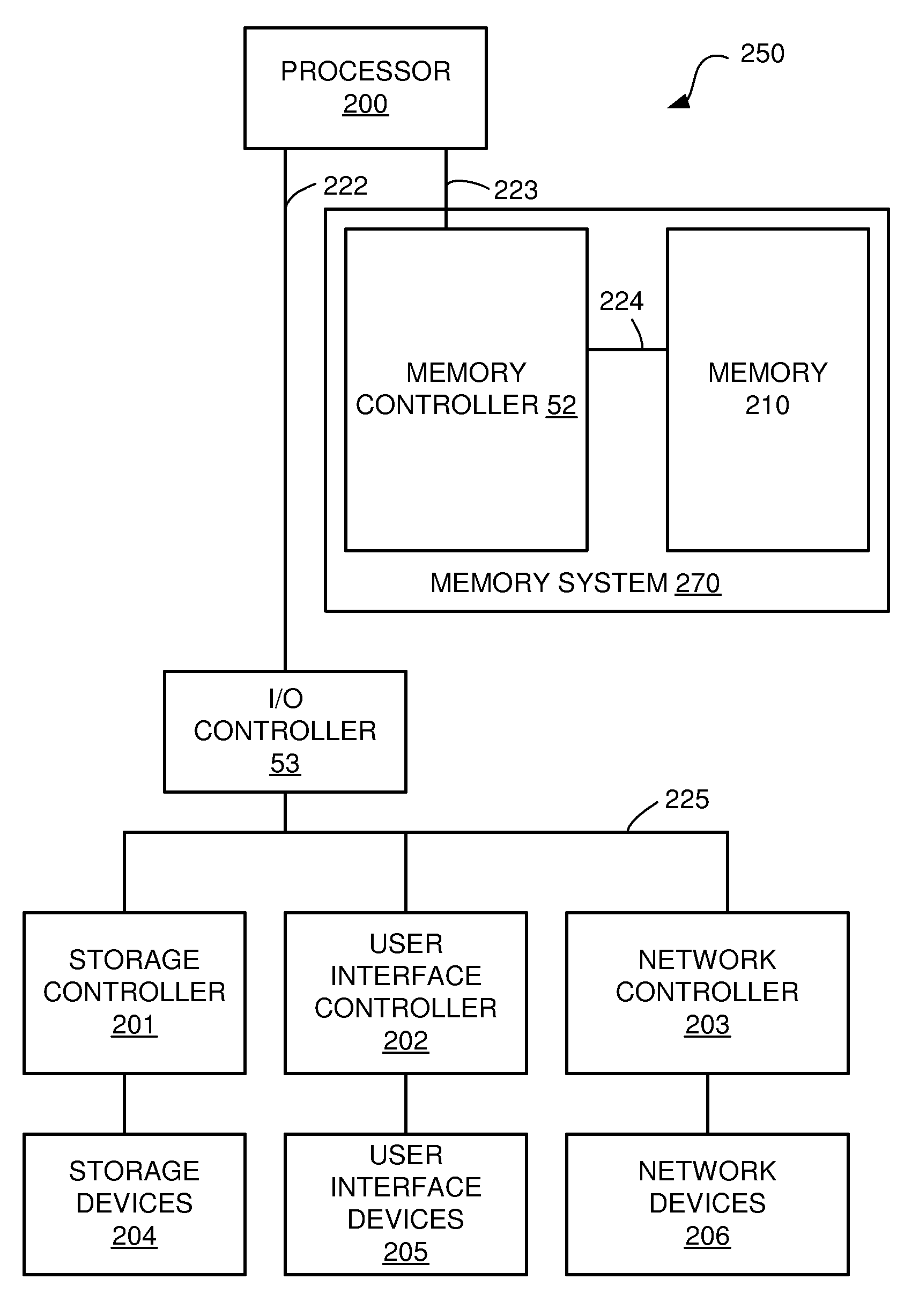
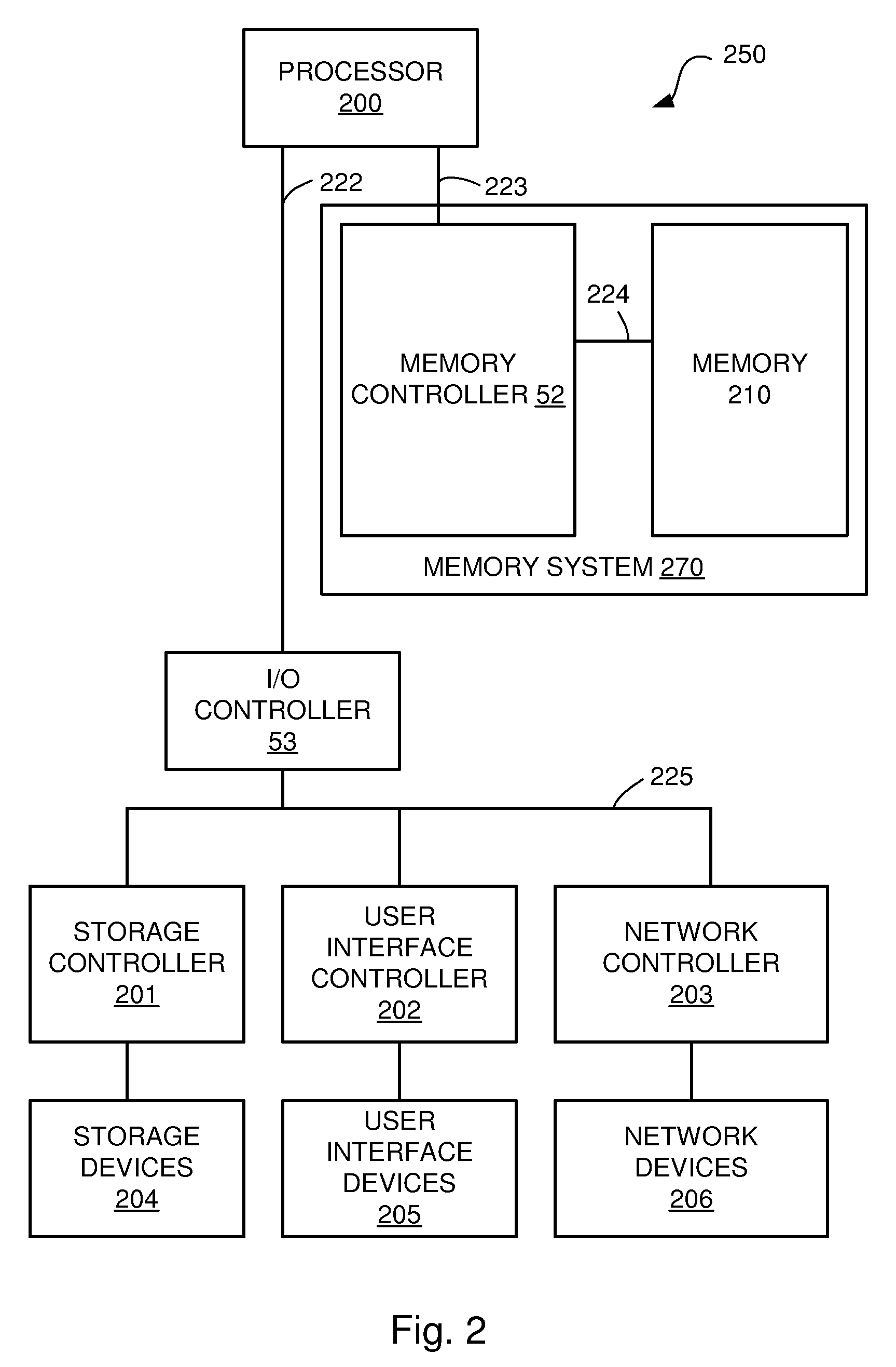
[0172]Embodiments of the invention are also expressed as methods. FIG. 14 is a high level flow chart of a method embodiment 700 of the invention. Method 700 begins at step 702. In step 704, a processor, such as processor 200 (FIG. 2) sends a request for a read or a write to a memory system such as memory system 270 in FIG. 2. The memory system further comprises a memory (memory 210) which further comprises one or more daisy chains of memory chips, the memory chips connected to the memory controller by a bus clock chain, an address / command bus chain, and a data bus chain.

[0173]In step 706, the memory controller sends a bus clock down a bus clock chain. The bus clock is received by a first memory chip in the daisy chain of memory chips, and is re-driven by the first memory chip to a second memory chip, and so on, through the daisy chain of memory chips. The bus clock is used to control how fast (i.e., at what frequency) address / command words and data words are transmitted on an addres...


PUM


Abstract

A memory chip suitable for use in a daisy chain of memory chips. The memory chip receives an address/command word on a first input, determines if the address command word is directed to the memory chip; if so, the memory chip accesses an array on the memory chip respondent to the address/command word. If not, the memory chip re-drives the address/command word on a first output. Write data is received as part of the address/command word or from a first data bus port. Read data is read from the array or is received from a second data bus port for subsequent re-driving on the first data bus port. A bus clock is received and is used to receive and transmit information on the first input, the first output, the first data bus port and the second data bus port.

Description

CROSS-REFERENCE TO RELATED APPLICATIONS[0001]This application is related to:[0002]U.S. application Ser. No. ______, filed on ______, 2006, Attorney Docket No. ROC920050364US1, entitled Daisy Chained Memory System.[0003]U.S. application Ser. No. ______, filed on ______, 2006, Attorney Docket No. ROC920060262US1, entitled Memory System Having Self Timed Daisy Chained Memory Chips.[0004]U.S. application Ser. No. _______, filed on _______, 2006, Attorney Docket No. ROC920060263US1, entitled Carrier Having Daisy Chained Memory Chips.[0005]U.S. application Ser. No. ______, filed on ______, 2006, Attorney Docket No. ROC920060264US1, entitled Carrier Having Daisy Chain of Self Timed Memory Chips.[0006]U.S. application Ser. No. ______, filed on ______, 2006, Attorney Docket No. ROC920060266US1, entitled Daisy Chainable Self Timed Memory Chip.[0007]U.S. application Ser. No. ______, filed on ______, 2006, Attorney Docket No. ROC920060267US1, entitled Computer System Having Daisy Chained Memory...

Claims


Application Information

Patent Timeline
Patent Type & Authority Applications(United States)
IPC IPC(8): G11C8/00
CPCG11C5/04G11C8/12G11C2029/3202G11C29/32G11C29/26
Inventor BARTLEY, GERALD KEITHBECKER, DARRYL JOHNDAHLEN, PAUL ERICGERMANN, PHILIP RAYMONDMAKI, ANDREW BENSONMAXSON, MARK OWEN
Owner GLOBALFOUNDRIES US INC
Why Eureka
Try Eureka