Multi-chip semiconductor memory device having internal power supply voltage generation circuit for decreasing current consumption

a semiconductor memory and voltage generation circuit technology, applied in the field of multi-chip semiconductor memory devices, can solve problems such as several limitations

Active Publication Date: 2007-04-12
SAMSUNG ELECTRONICS CO LTD
View PDF7 Cites 111 Cited by
  • Summary
  • Abstract
  • Description
  • Claims
  • Application Information

AI Technical Summary

Problems solved by technology

While the conventional multi-chip semiconductor memory device includes a plurality of memory chips, it has several limitations.

Method used


Image

  • Multi-chip semiconductor memory device having internal power supply voltage generation circuit for decreasing current consumption
  • Multi-chip semiconductor memory device having internal power supply voltage generation circuit for decreasing current consumption
  • Multi-chip semiconductor memory device having internal power supply voltage generation circuit for decreasing current consumption

Examples


Embodiment Construction

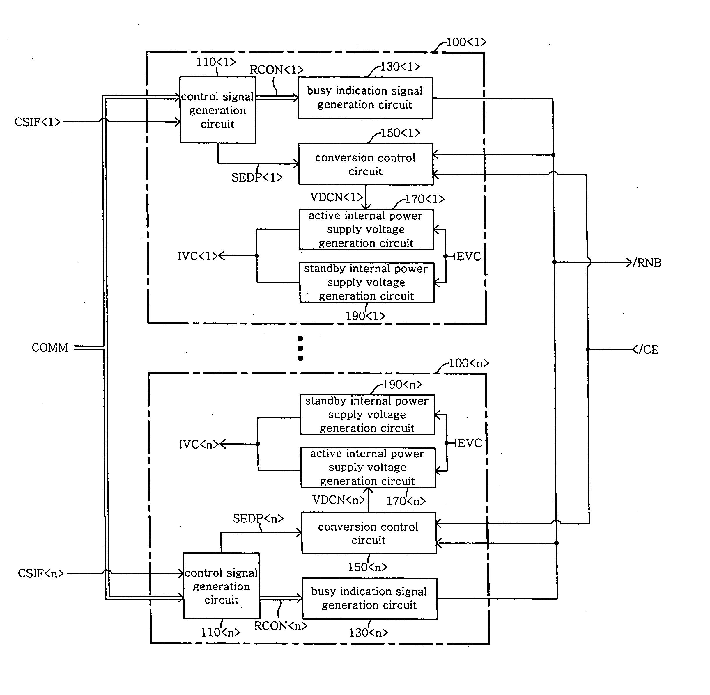
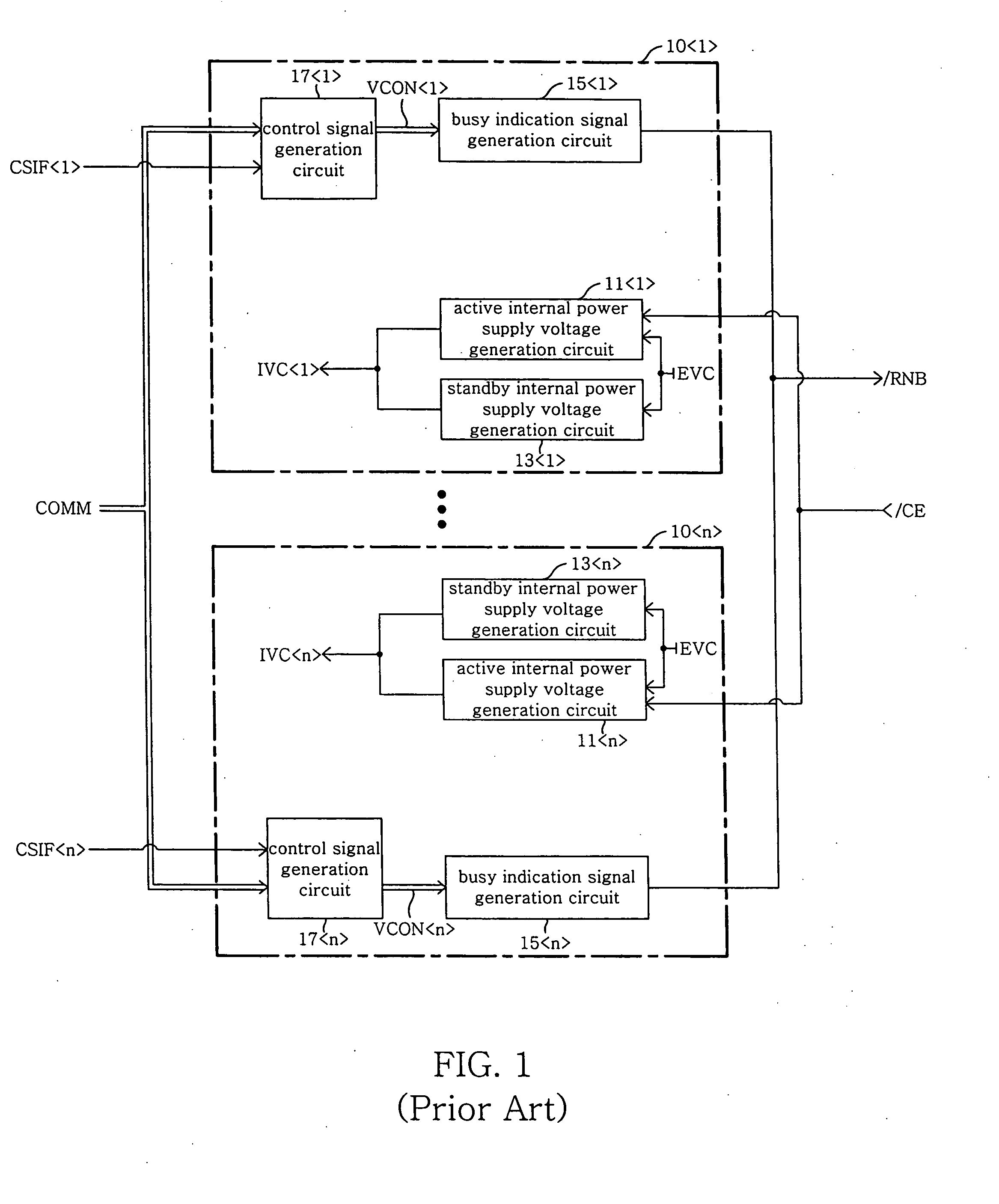
[0020] Reference should now be made to the drawings, in which the same reference numerals are used throughout the different drawings to designate the same or similar components.

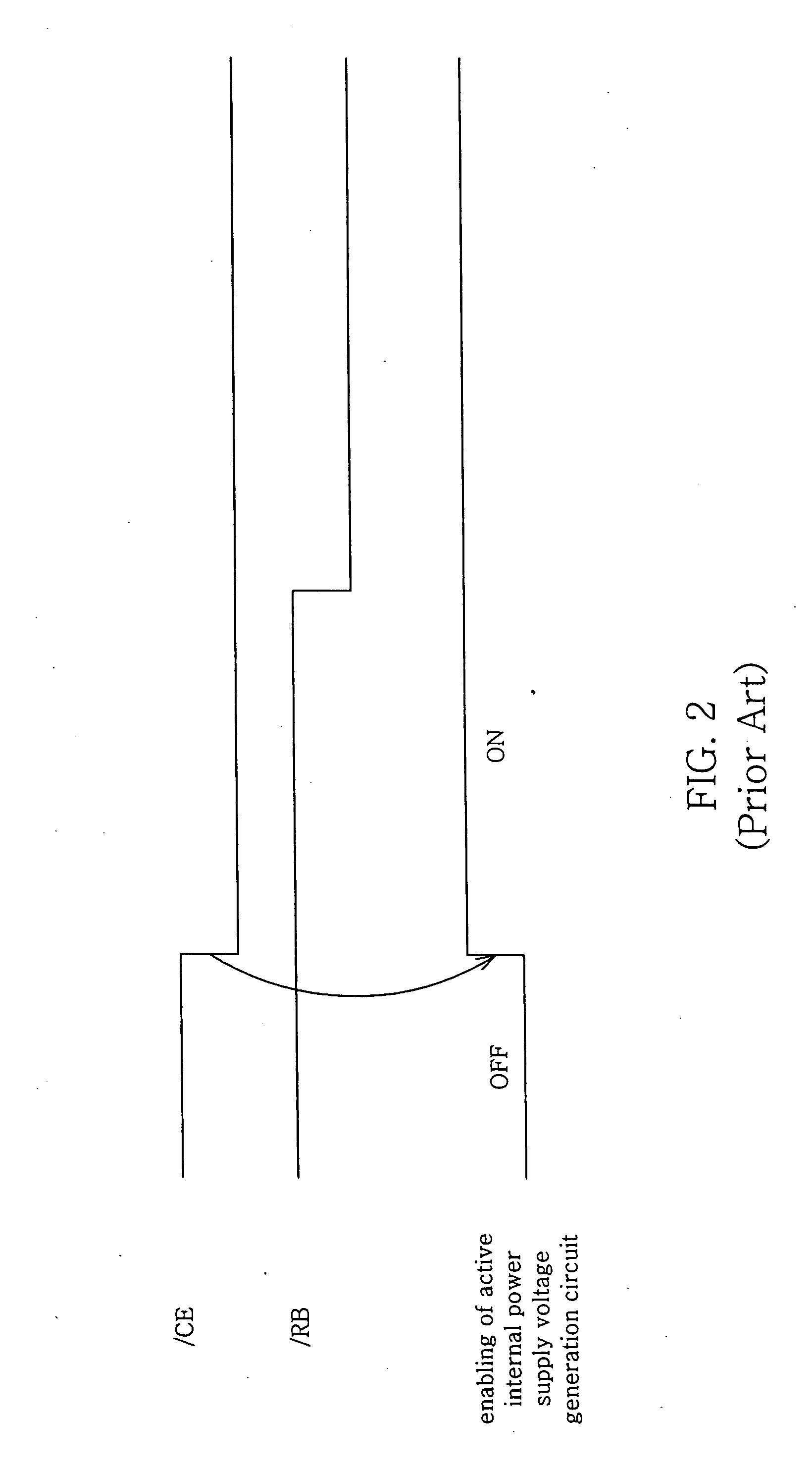
[0021] In the present specification, a memory cell may perform a program or erase operation using the data of the data line of a corresponding memory chip, or may perform a read operation, in which the data of a memory cell is read to a data line during a ‘busy interval.’ Furthermore, a ‘command input operation’ in which a command is received from a corresponding memory chip, may be performed during a ‘command input interval.’

[0022] In the present specification, the ‘busy operation’ and the ‘command input operation’ may be referred to in common as an “active operabon”, and the ‘busy interval’ and the ‘command input interval’ may be referred to in common as an “active interval.”

[0023] In the present specification, embodiments in which a plurality of memory chips are implemented using “nonvolatile memory” are ...


PUM


Abstract

A multi-chip semiconductor memory device may comprise of a plurality of memory chips sharing a predetermined chip enable signal. Each of the plurality of memory chips may comprise of an active internal power supply generation circuit configured to convert an external power supply voltage into an internal power supply voltage and to be disabled in response to deactivation of a predetermined drive control signal. Each of the plurality of memory chips may also comprise of a conversion control circuit for generating the drive control signal, wherein the drive control signal is deactivated in an interval in which any of the plurality of memory chips is in an active interval.

Description

BACKGROUND OF THE INVENTION [0001] 1. Field of the Invention [0002] The present invention relates generally to a multi-chip semiconductor memory device having a plurality of memory chips, and more particularly, to a multi-chip semiconductor memory device having a plurality of memory chips, each including internal power supply voltage generation circuits which independently convert an external power supply voltage into an internal power supply voltage. [0003] 2. Description of the Related Art [0004] A memory chip includes an internal power supply voltage generation circuit which may generate a low-level internal power supply voltage by converting an external power supply voltage into the internal power supply voltage. Power consumption of the memory chip may be decreased by using such an internal power supply voltage generation circuit. Furthermore, even though the external power supply voltage may change, the internal power supply voltage may be kept relatively uniform, so that the ...

Claims


Application Information

Patent Timeline
Patent Type & Authority Applications(United States)
IPC IPC(8): G11C5/14
CPCG11C5/04G11C5/143G11C5/144G11C7/22G11C16/30
Inventor KWON, OH SUKBYEON, DAE SEOK
Owner SAMSUNG ELECTRONICS CO LTD
Why Eureka
Try Eureka