Semiconductor device and a method of manufacturing the same

a technology of semiconductors and devices, applied in semiconductor/solid-state device testing/measurement, instruments, nanoinformatics, etc., can solve the problems of difficult to detect the existence of short circuit between the wires, and difficult to reduce the thickness of the package, so as to reduce the distance between the wire and the wire directly, the effect of increasing the loop height of the wir

Inactive Publication Date: 2006-06-13
LONGITUDE LICENSING LTD
View PDF18 Cites 118 Cited by
  • Summary
  • Abstract
  • Description
  • Claims
  • Application Information

AI Technical Summary

Benefits of technology

[0007]Among the plurality of wires for connecting the electrically common bonding pad with an electrode, the wire to be connected with the bonding pad of the lower semiconductor chip lies almost directly under the wire to be connected with the bonding pad of the upper semiconductor chip. Lowering the loop height of the wire to be connected with the bonding pad of the upper semiconductor chip therefore reduces the distance between the wire and a wire directly thereunder, which tends to cause a short circuit between these wires. An increase in the loop height of the wire to be connected with the bonding pad of the upper semiconductor chip to prevent such a phenomenon, on the other hand, thickens the resin provided for sealing the semiconductor chip and wire, thereby making it difficult to reduce the thickness of the package.
[0008]An object of the present invention is to provide a technique for improving the reliability of the visual inspection conducted after a wire bonding step, in a semiconductor device having a plurality of semiconductor chips stacked on one another and sealed with a resin.
[0009]Another object of the present invention is to provide a technique for promoting a size and thickness reduction of a semiconductor device having a plurality of semiconductor chips stacked on one another and sealed with a resin.
[0010]A further object of the present invention is to provide a technique for reducing the manufacturing cost of a semiconductor device having a plurality of semiconductor chips stacked on one another and sealed with a resin.

Problems solved by technology

If at least two semiconductor chips, which are similar in size and in the position of a bonding pad thereof, are mounted, and the bonding pad of each of the semiconductor chips is connected with an electrode of the substrate by a wire, it becomes difficult to detect the existence of a short circuit between the wires in a visual inspection step conducted after completion of the wire bonding step, because a plurality of wires for connecting each of the electrically common bonding pads of these semiconductor chips with an electrode seem to overlap when viewed downwards from above.
Lowering the loop height of the wire to be connected with the bonding pad of the upper semiconductor chip therefore reduces the distance between the wire and a wire directly thereunder, which tends to cause a short circuit between these wires.
An increase in the loop height of the wire to be connected with the bonding pad of the upper semiconductor chip to prevent such a phenomenon, on the other hand, thickens the resin provided for sealing the semiconductor chip and wire, thereby making it difficult to reduce the thickness of the package.

Method used


Image

  • Semiconductor device and a method of manufacturing the same
  • Semiconductor device and a method of manufacturing the same
  • Semiconductor device and a method of manufacturing the same

Examples


embodiment 1

[0040](Embodiment 1)

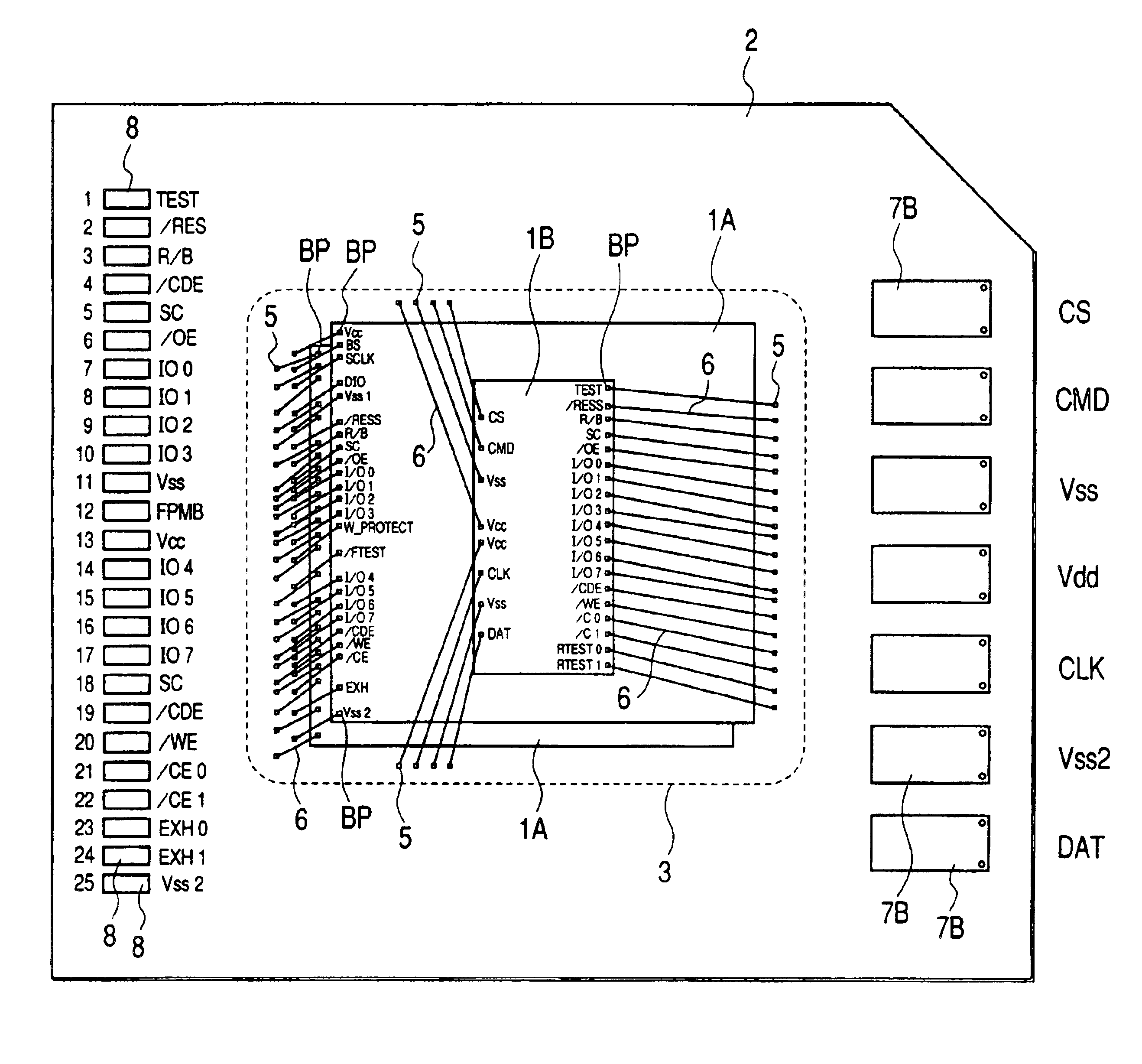
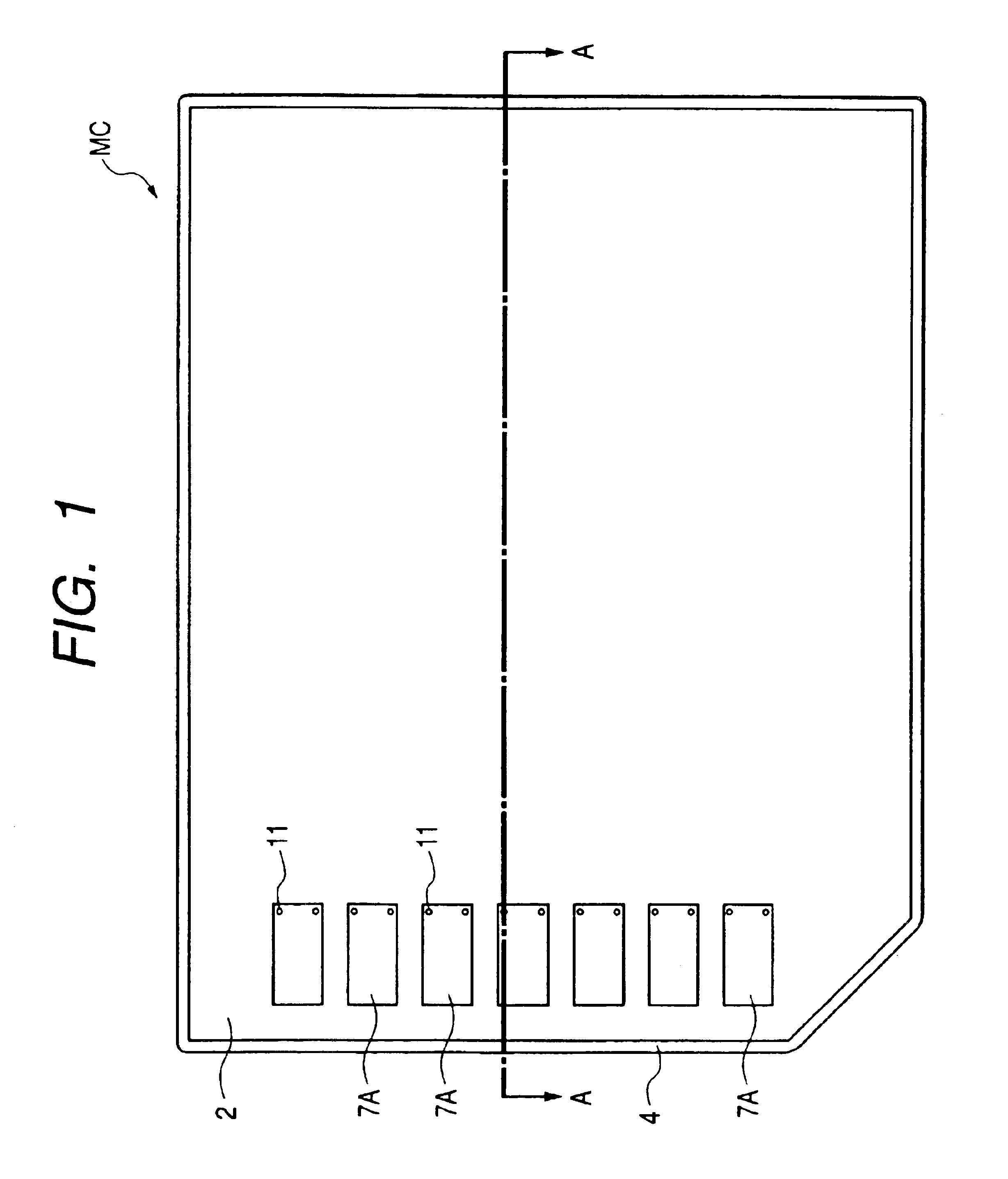
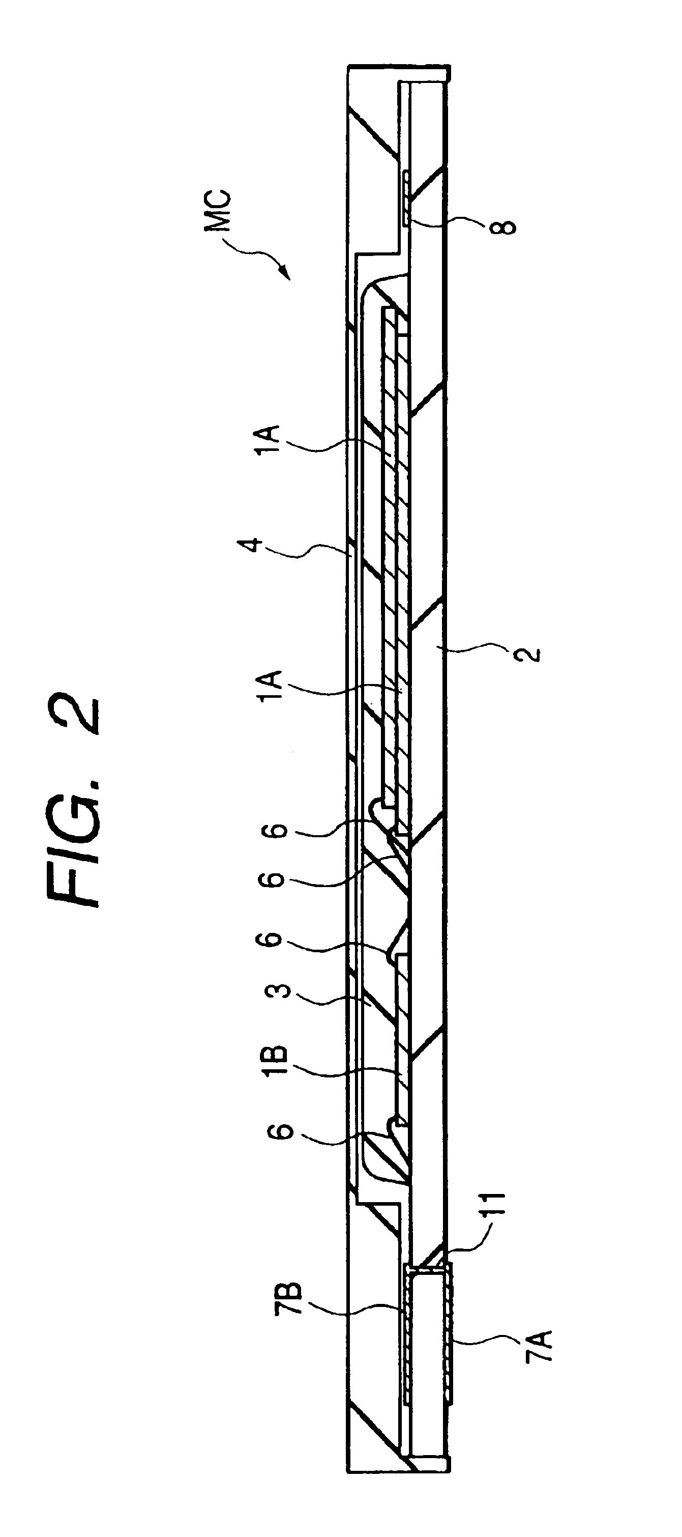
[0041]FIG. 1 is a plan view illustrating the outer appearance of the semiconductor device according to this Embodiment; FIG. 2 is a cross-sectional view taken along the longitudinal direction (a line A—A) of this semiconductor device; and FIG. 3 is a plan view illustrating the base substrate of this semiconductor device.

[0042]The semiconductor device according to this Embodiment is a memory card MC which is obtained by mounting, over a base substrate 2, two semiconductor chips (which will hereinafter be called chips or memory chips) 1A having, over the main surface thereof, a flash memory formed as a semiconductor element and a semiconductor chip (which will hereinafter be called a chip or control chip) 1B having a control circuit for the flash memory formed thereon; sealing these three chips 1A, 1A and 1B with a resin 3; and then, covering the upper surface of the base substrate 2 with a resin-made cap 4. This memory card MC is used for storing data, such as ima...

embodiment 2

[0061](Embodiment 2)

[0062]FIG. 13 is a cross-sectional view illustrating the semiconductor device of this Embodiment, while FIG. 14 is a plan view illustrating the base substrate of this semiconductor device.

[0063]The semiconductor device of this Embodiment is a memory card MC obtained by mounting over a base substrate 2 four memory chips 1A1 to 1A4, each having a flash memory formed thereon, and a control chip 1B; sealing these chips 1A1 to 1A4 and 1B with a resin 3; and covering the upper surface of the base substrate 2 with a resin cap 4.

[0064]The four memory chips 1A1 to 1A4 have the same external size and have a flash memory of the same memory capacity formed thereon. These memory chips 1A1 to 1A4 each have a single-side pad system wherein bonding pads BP are formed at the periphery of the element surface, and they are arranged in a line along one of the sides of each of the memory chips.

[0065]In this Embodiment, these four memory chips 1A1 to 1A4 are mounted over the base subs...


PUM


Abstract

Two memory chips mounted over a base substrate have the same external size and a flash memory of the same memory capacity formed thereon. These memory chips are mounted over the base substrate with one of them being overlapped with the upper portion of the other one, and they are stacked with their faces being turned in the same direction. The bonding pads BP of one of the memory chips are disposed in the vicinity of the bonding pads BP of the other memory chip. In addition, the upper memory chip is stacked over the lower memory chip in such a way that the upper memory chip is slid in a direction (X direction) parallel to the one side of the lower memory chip and in a direction (Y direction) perpendicular thereto in order to prevent partial overlapping of it with the bonding pads BP of the lower memory chip.

Description

[0001]This application is a Division of U.S. application Ser. No. 10 / 194,224, filed Jul. 15, 2002, now U.S. pat. No. 6,686,663, which, in turn, is a Continuation of U.S. application Ser. No. 09 / 769,359, filed Jan. 26, 2001, now U.S. Pat. No. 6,538,331, the entire disclosures of which are hereby incorporated by reference.FIELD OF THE INVENTION[0002]The present invention relates to a semiconductor device, and to a technique for manufacturing the same; and, more particularly, the invention relates to a technique which is effective when applied to a semiconductor device having a plurality of semiconductor chips stacked therein, and which is resin-sealed in a single package.BACKGROUND OF THE INVENTION[0003]As one of the measures for increasing the capacity of a memory LSI, such as a flash memory or a DRAM (dynamic random access memory), a variety of memory module structures, which are manufactured by stacking semiconductor chips, each having such a memory LSI formed thereon, and then sea...

Claims


Application Information

Patent Timeline
Patent Type & Authority Patents(United States)
IPC IPC(8): H01L23/34H01L25/18H01L21/60H01L23/31H01L25/065H01L25/07
CPCB82Y10/00H01L25/0652G06K19/07732H01L23/3128H01L22/32H01L23/5388H01L24/49G11C5/02H01L23/50H01L23/3121G06K19/077H05K1/117H01L25/0657H01L25/074H01L24/06H01L2224/45144H01L2924/15311H01L2924/01013H01L2225/06562H01L2224/49171H05K1/0268H01L2924/01033H05K2203/1572H01L2924/01079H01L2924/01005H01L2924/01039H01L2924/01004H01L2224/48091H05K2201/10159H01L2224/32145H01L2224/48227H01L2224/73265H01L2225/0651H01L24/48H01L2924/14H01L2224/49113H01L24/45H01L2924/1815H01L2924/01006H01L2924/01057H01L2924/014H05K3/284H01L2224/32225H01L2224/04042H01L2924/01082H01L2924/00014H01L2924/00H01L2924/00012H01L24/73H01L2224/05554H01L2924/181H01L2924/351H01L21/60
Inventor MASUDA, MASACHIKAUSAMI, TOSHIHIKO
Owner LONGITUDE LICENSING LTD
Why Eureka
Try Eureka