

Exposure Method, Exposure Apparatus, Exposure System and Device Manufacturing Method
a technology of exposure apparatus and manufacturing method, applied in the direction of photomechanical apparatus, instruments, printing, etc., can solve the problems of reducing throughput and generally requiring a relatively longer time for exposure of exposure apparatus, and achieve the effect of high throughput, high accuracy and high accuracy
- Summary
- Abstract
- Description
- Claims
- Application Information
AI Technical Summary
Benefits of technology
Problems solved by technology
Method used
Image

Examples
first embodiment
A FIRST EMBODIMENT
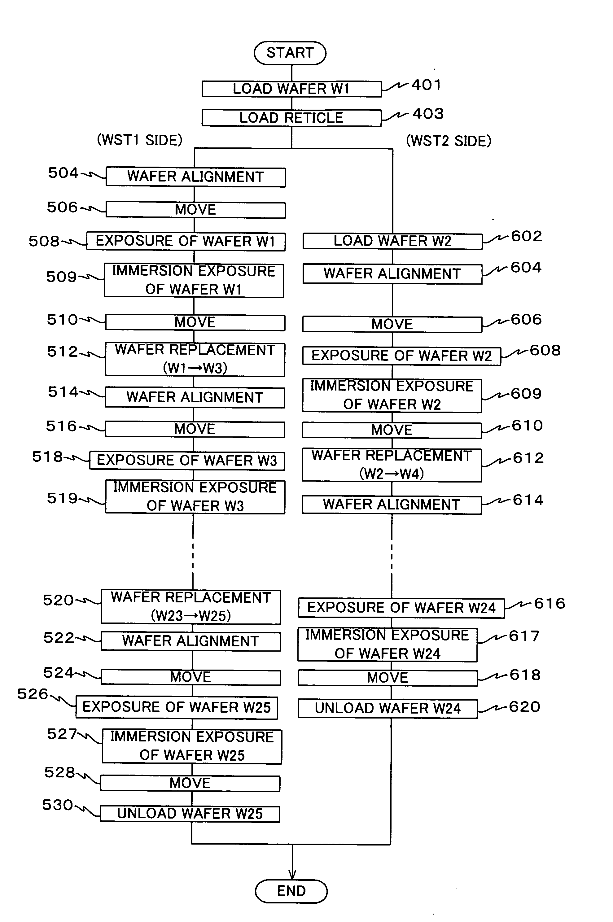
[0036]A first embodiment of the present invention will be described below, referring to FIGS. 1 to 10; however, the present invention is not limited to this.
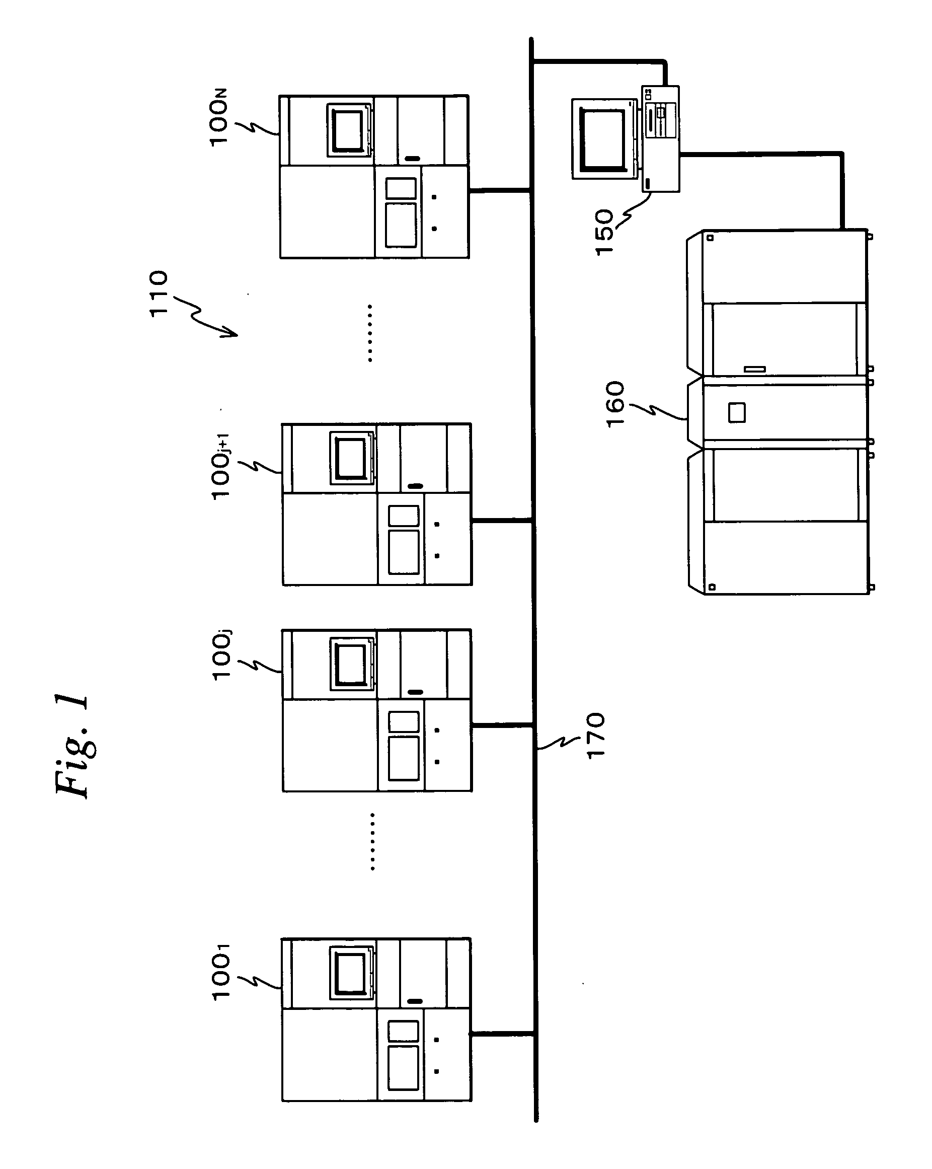
[0037]FIG. 1 schematically shows the configuration of a lithography system 110 serving as an exposure system related to the first embodiment of the present invention. Lithography system 110 includes N units of exposure apparatus (1001to 100N), a terminal server 150, a host computer system 160 and the like. Of these parts, each exposure apparatus 100i (i=1, 2, . . . , j, j+1, . . . , N) and terminal server 150 connect to a local area network (LAN) 170, and the host computer system 160 connects to terminal server 150. Further, a communication path is secured between exposure apparatus (1001 to 100N) and host computer system (hereinafter, simply referred to as a “host”) 160, and communication between host 160 and exposure apparatus (1001 to 100N) is performed using the communication path.
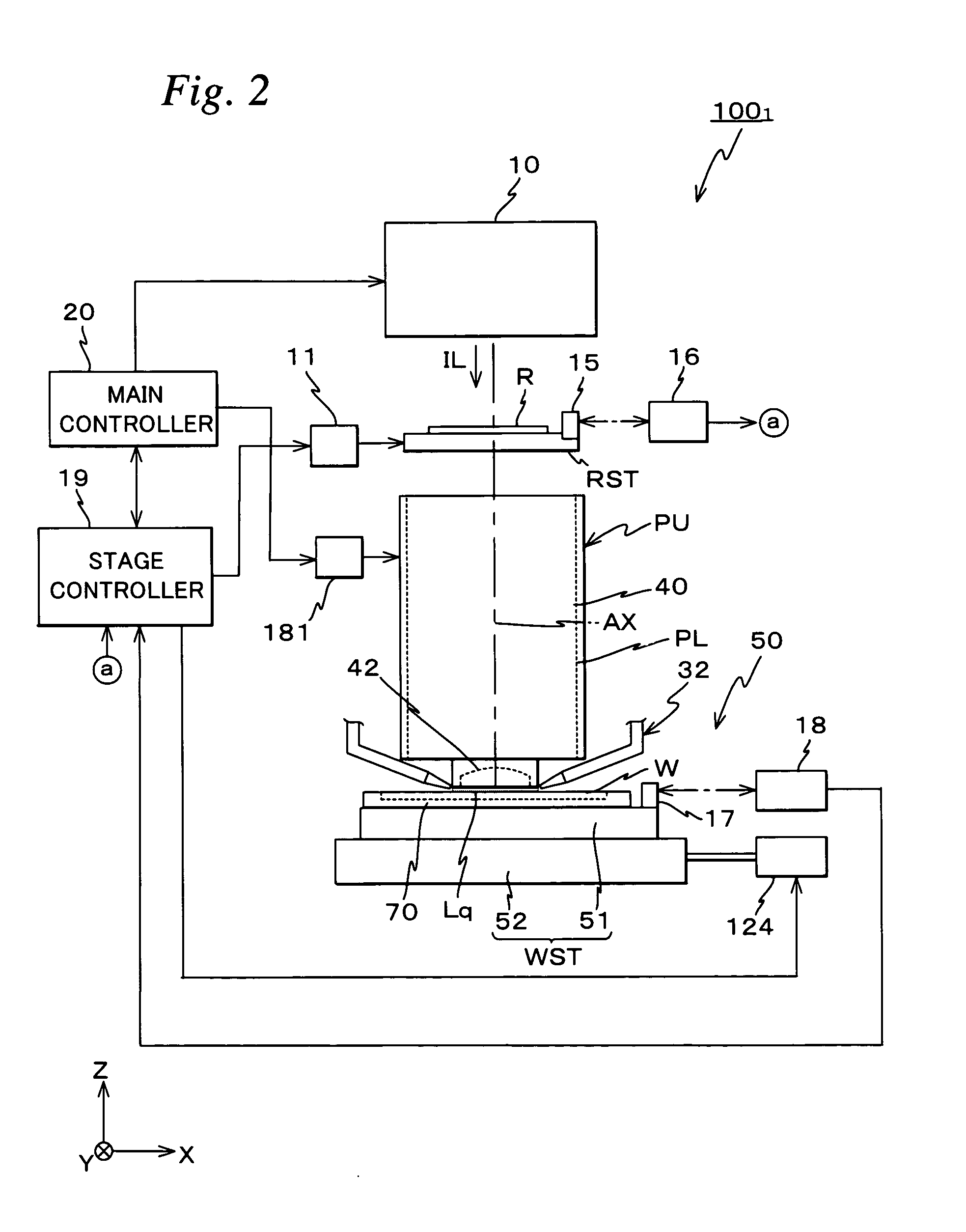
[0038]Exposure apparatus (...
second embodiment
A SECOND EMBODIMENT
[0138]Next, a second embodiment of the present invention will be described, referring to FIGS. 11 to 14. In the first embodiment above, double exposure was performed using two different exposure apparatus, however, in the second embodiment, double exposure using reticle 9A and reticle 9B described above in one exposure apparatus will be performed.
[0139]FIG. 11 shows a schematic configuration of an exposure apparatus 100 related to the second embodiment of the present invention. Exposure apparatus 100 is a so-called step-and-scan exposure apparatus (scanning stepper). Exposure apparatus 100 is an exposure apparatus that can perform exposure by the immersion method similar to exposure apparatus 1001 of the first embodiment, and is equipped with a liquid supply / drainage system 32. Exposure apparatus 100 is configured in a similar manner as exposure apparatus 1001 except for the point that it is equipped with a projection optical system PL′ instead of projection optic...
PUM
| Property | Measurement | Unit |
|---|---|---|
| refractive index | aaaaa | aaaaa |
| wavelength | aaaaa | aaaaa |
| wavelength | aaaaa | aaaaa |
Abstract
Description
Claims
Application Information