Making LCD panel alignment layers and spacers

Active Publication Date: 2008-02-28
SAMSUNG DISPLAY CO LTD
View PDF1 Cites 29 Cited by
  • Summary
  • Abstract
  • Description
  • Claims
  • Application Information

AI Technical Summary

Benefits of technology

[0016]A better understanding of the above and many other features and advantages of the methods and apparatus of the present invention, as well as LCD panels manufactured using such methods and apparatus, may be obtained from a consideration of the detailed d

Problems solved by technology

However, the photolithography process has a number of drawbacks, including that it requires a long time to complete, is wasteful of the photoresist stripping solution, and requires large, expensive photolithography equipment, the size and cost of which escalate dramatically as LCD panel sizes increase and pattern sizes decrease.

Method used


Image

  • Making LCD panel alignment layers and spacers
  • Making LCD panel alignment layers and spacers
  • Making LCD panel alignment layers and spacers

Examples


Embodiment Construction

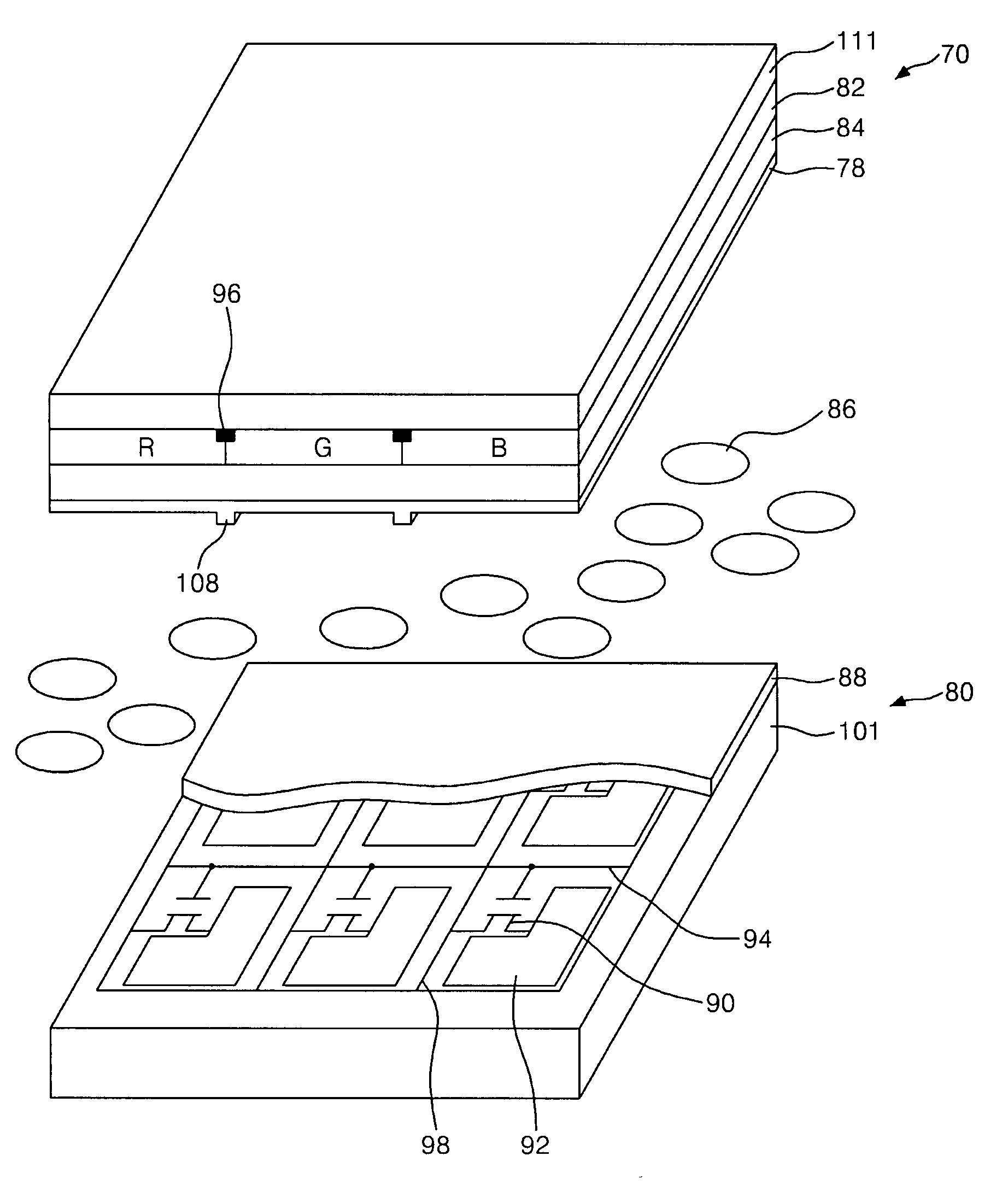
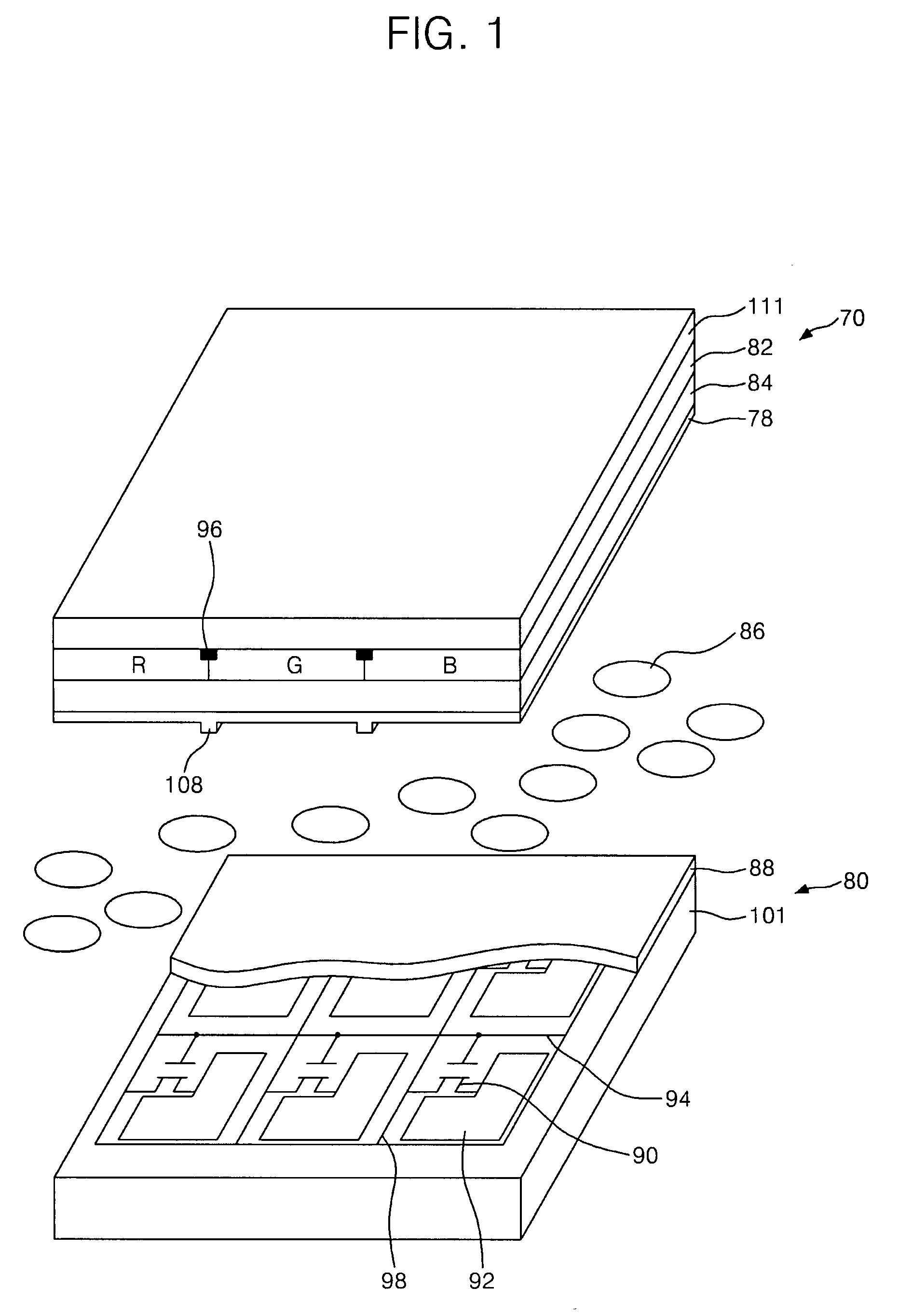
[0021]FIG. 1 is schematic exploded upper front and side perspective view of an exemplary embodiment of an LCD panel manufactured in accordance with the methods and apparatus of the present invention. As illustrated in FIG. 1, the LCD panel includes a color filter substrate 70 and a thin film transistor (TFT) substrate 80 in disposed in facing abutment with each other, with a layer of a liquid crystal 86 material sealed between the two substrates 70, 80.

[0022]The color filter substrate 70 includes, in descending order, an upper substrate 111 having a black matrix 96, a plurality of color filters 82, a common electrode 84, and an upper alignment layer 78 having a plurality of column spacers 108 integrally formed thereon. The black matrix 96 is formed on a lower surface of the upper substrate 111 and serves to divide the upper substrate 111 into a plurality of cell regions in which the color filters 82 are respectively formed, and also serves to protect against optical interference bet...


PUM


Abstract

Methods and apparatus are described for forming an alignment layer and integral spacers on an LCD substrate simultaneously using a non-photolithographic imprinting process and for manufacturing LCD panels incorporating such substrates. One method includes forming a first alignment layer and a plurality of integral spacers simultaneously and of the same material on one LCD substrate, forming a second alignment layer on the other substrate, and arranging the two substrates such that the two alignment layers are disposed in facing opposition to each other, with the spacers interposed therebetween.

Description

RELATED APPLICATIONS[0001]This application claims priority of Korean patent application 2006-69685, filed Jul. 25, 2006, the entire disclosure of which is incorporated herein by reference.BACKGROUND[0002]This disclosure relates to liquid crystal displays (LCDs) in general, and in particular, to methods and apparatus for simultaneously forming LCD panel alignment layers and integral column spacers with a non-photolithographic patterning process.[0003]In an effort to address the relatively large size and weight penalties of conventional Cathode Ray Tube (CRT) displays, a variety of flat panel display types, including LCDs, plasma display panels (PDPs), field emission displays (FEDs), and light emitting diode displays (LEDDs) have recently been researched and developed as substitutes therefor, all of which are thinner, lighter and occupy less volume than comparable CRT displays.[0004]The display panel of an LCD produces an image by adjusting the light transmittance of the molecules of ...

Claims


Application Information

Patent Timeline
IPC IPC(8): G02F1/1337G02F1/13G02F1/1339
CPCG02F1/13394G02F1/1337G02F1/1339
Inventor KIM, SANG II
Owner SAMSUNG DISPLAY CO LTD
Why Eureka
Try Eureka