Non-Volatile Memory Cell In Standard CMOS Process

Active Publication Date: 2008-03-06
SEMICON COMPONENTS IND LLC
View PDF14 Cites 8 Cited by
  • Summary
  • Abstract
  • Description
  • Claims
  • Application Information

AI Technical Summary

Benefits of technology

[0010]To perform a read operation, the flip-flop circuit is reset to a first logic state. If the floating gate has been erased to store a positive charge, the NMOS transistor will turn on in response to this stored positive charge, thereby switching the state of the flip-flop circuit to a second logic state. Conversely, if the floating gate has been programmed to store a negative charge, the NMOS transistor will be turned off in response to this negative charge, thereby leaving the flip-flop circuit in the first logic state. No current paths exist during the read operation, thereby minimizing power consumption during the read operation.

Problems solved by technology

Finally, non-volatile memory circuit 100 does not provide for a margin read operation to test the reliability of the circuit.
Consequently, memory circuit 100 will exhibit low reliability / quality.
In addition, the '574 patent does not provide for a margin read operation to test the reliability of non-volatile memory cell 200.
(Indeed, the '574 patent does not provide details of the read circuitry used to access non-volatile memory cell 200.)
Consequently, non-volatile memory cell 200 will exhibit low reliability / quality.
Non-volatile memory element 300 implements destructive (one-time only) programming, which severely limits the use of this element.
Moreover, shorting the gate oxide typically requires significant current and power consumption.

Method used


Image

  • Non-Volatile Memory Cell In Standard CMOS Process
  • Non-Volatile Memory Cell In Standard CMOS Process
  • Non-Volatile Memory Cell In Standard CMOS Process

Examples


Embodiment Construction

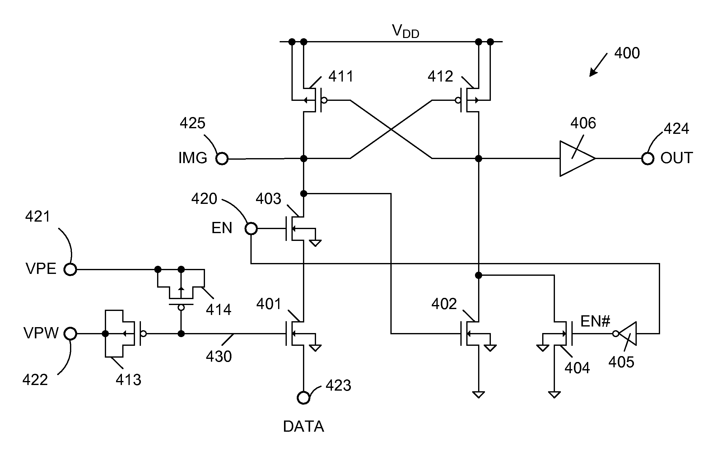
[0018]FIG. 4 is a circuit diagram of a non-volatile memory (NVM) cell 400 in accordance with one embodiment of the present invention. NVM cell 400 includes n-channel (NMOS) field effect transistors 401-404, inverter 405, output buffer 406, p-channel (PMOS) field effect transistors 411-414 and signal nodes 420-425.

[0019]The sources and n-type body regions of p-channel transistors 411 and 412 are commonly connected to receive a positive supply voltage VDD. The gate of p-channel transistor 412 is coupled to the drain of p-channel transistor 411, current injection node 425, and the gate of n-channel transistor 402. The gate of p-channel transistor 411 is coupled to the drain of p-channel transistor 412, the drains of n-channel transistors 402 and 404, and the input terminal of output buffer 406. The output terminal of output buffer 406 is coupled to NVM cell output node 424.

[0020]N-channel transistors 401 and 403 are connected in series between the drain of p-channel transistor 411 and ...


PUM


Abstract

A non-volatile memory cell fabricated with a conventional CMOS process, including a flip-flop circuit having an NMOS transistor that shares a floating gate with a write PMOS capacitor and an erase PMOS capacitor. An erase function is implemented by inducing Fowler-Nordheim tunneling through the erase PMOS capacitor, thereby providing a positive charge on the floating gate. A write function is implemented by inducing Fowler-Nordheim tunneling through the NMOS transistor, thereby providing a negative charge on the floating gate. The write PMOS capacitor provides bias voltages during the erase and write operations. Prior to a read operation, the flip-flop circuit is reset. If the floating gate stores a positive charge, the NMOS transistor turns on, thereby switching the state of the flip-flop circuit. If the floating gate stores a negative charge, the NMOS transistor turns off, thereby leaving the flip-flop circuit in the reset state.

Description

BACKGROUND OF THE INVENTION[0001]1. Technical Field[0002]The present invention is in the field of non-volatile programmable integrated circuits using standard CMOS technology.[0003]2. Related Art[0004]FIG. 1 is a circuit diagram of a conventional differential floating gate non-volatile memory circuit 100, which includes p-channel (PMOS) field effect transistors 101-105 and differential sense amplifier 106. Non-volatile memory circuit 100 uses a differential configuration, wherein a data bit is represented by the charge stored on the two floating nodes FG0 and FG1. Non-volatile memory circuit 100 is described in more detail in U.S. Pat. No. 6,950,342. Non-volatile memory circuit 100 is a complex circuit that requires a large per-bit layout area. Moreover, non-volatile memory circuit 100 requires at least 4-5 current branches to enable program, erase and read operations. Finally, non-volatile memory circuit 100 does not provide for a margin read operation to test the reliability of th...

Claims


Application Information

Patent Timeline
IPC IPC(8): G11C11/24
CPCG11C16/0441
Inventor EFTIMIE, SABIN A.POENARU, ILIE MARIAN I.GEORGESCU, SORIN S.
Owner SEMICON COMPONENTS IND LLC
Why Eureka
Try Eureka