Method for fabricating semiconductor

Inactive Publication Date: 2008-04-03
LAPIS SEMICON CO LTD
View PDF6 Cites 3 Cited by
  • Summary
  • Abstract
  • Description
  • Claims
  • Application Information

AI Technical Summary

Benefits of technology

[0015]In a silicon ion implantation, by reducing the number of interstitial Si in the proximity of the surface of a silicon layer having crystalline defects below 6.5E21/cm3 and increasing an ion dose per unit area into the proximity of the interface between the sapphire substrate and the silicon layer to 3.0E19 ions/cm3 or more, crystalline defects in an epitaxially grown silicon layer can be reduced, thereby improving device characteristics.
[0016]Silicon ion implantation into a silicon layer under the condition of a dosage of 8E14 ions/cm2 to 8.5E14 ions/cm2 can attain an ion dose per unit area into the proximity of the interface between the sapphire substrate and the silicon layer of 3.0E19 ions/cm3 or more. This can induce the silicon layer to become amorphous sufficiently in the proximity of the interface with the sapphire substrate and suppress the silicon layer from becoming amorphous in the proximity of the surface of the silicon layer a

Problems solved by technology

A silicon film may have a crystalline defect due to the crystal and thermal expansion incoherency between silicon and sapphire.
Unfortunately, crystalline defects in a silicon epitaxial layer adversely affect device characteristics and hence deteriorate device performance (speed).
Unfortun

Method used


Image

  • Method for fabricating semiconductor
  • Method for fabricating semiconductor
  • Method for fabricating semiconductor

Examples


first embodiment

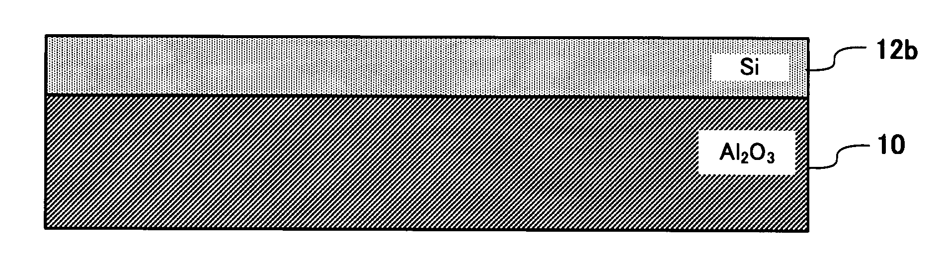
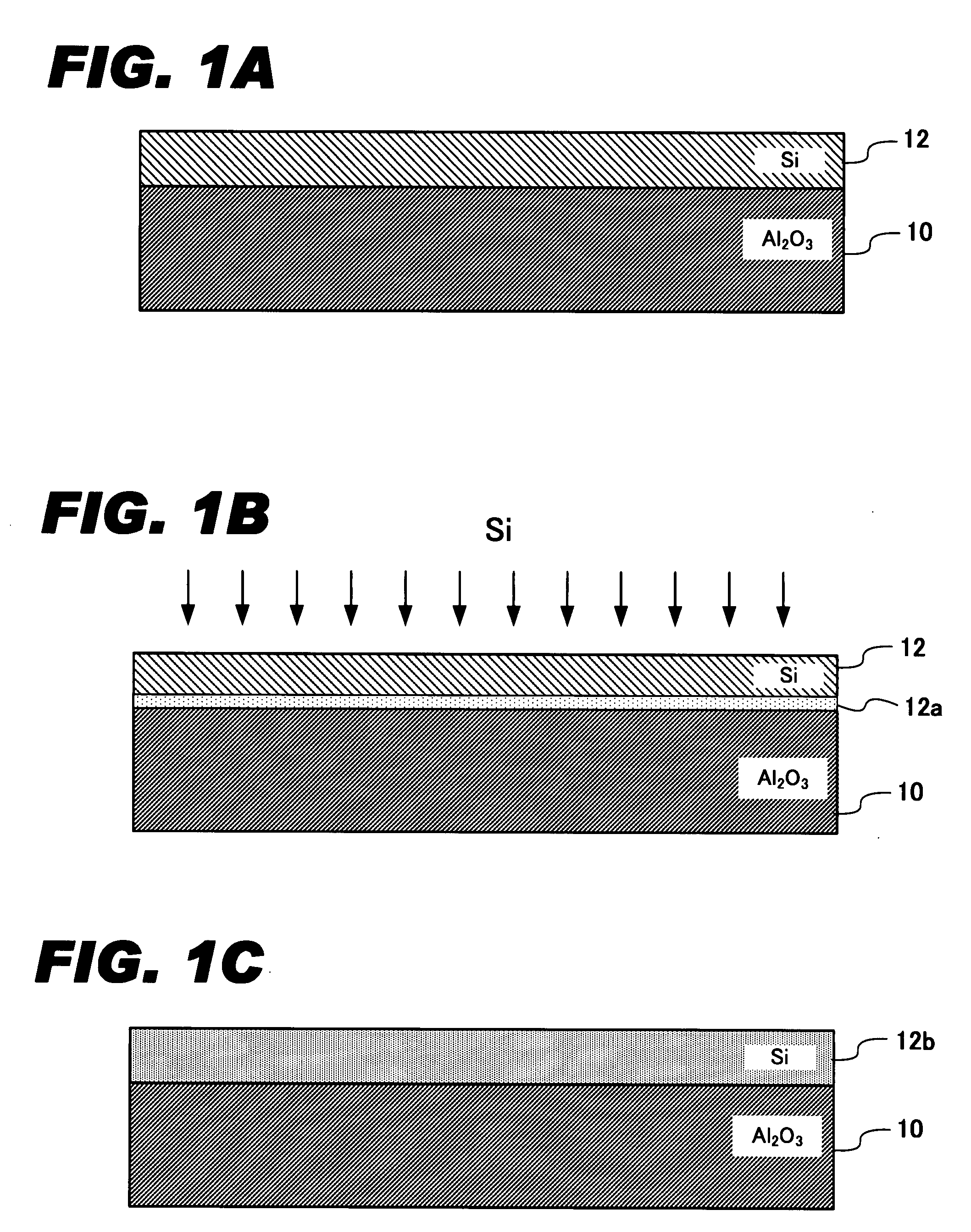
[0039]FIGS. 1A to 1C are cross-sectional views of an SOS wafer schematically showing a part of fabrication steps of the SOS wafer according to the present invention.

[0040]As shown in FIG. 1A, a silicon layer 12 having a thickness of approx. 2800 Å on a sapphire substrate. Next as shown in FIG. 1B, silicon ions are implanted into the silicon layer 12 to induce an amorphous region 12a to be formed in the proximity of the interface with the sapphire substrate 10. Then as shown in FIG. 1C, the silicon layer is epitaxially regrown (12b). The present invention applies to the process shown in FIG. 1B and provides optimized conditions for silicon ion implantation so as to suppress defects in the epitaxially grown silicon layer 12b.

[0041]The first embodiment of the present invention provides an optimized dosage (density: the number of ions per unit area) for Si implantation into the silicon layer 12. In practice in this embodiment, the conditions of a dosage of 8E14 / cm2 (±10%) and implantat...

second embodiment

[0049]The second embodiment of the present invention provides optimized implantation energy for Si implantation into the silicon layer 12. In practice in this embodiment, the conditions of a dosage of 6E14 / cm2 (±10%) and implantation energy of 160 KeV to 140 Kev are employed for silicon ion implantation, instead of the conventional conditions of a dosage of 6E14 / cm2 and implantation energy of 185 Kev.

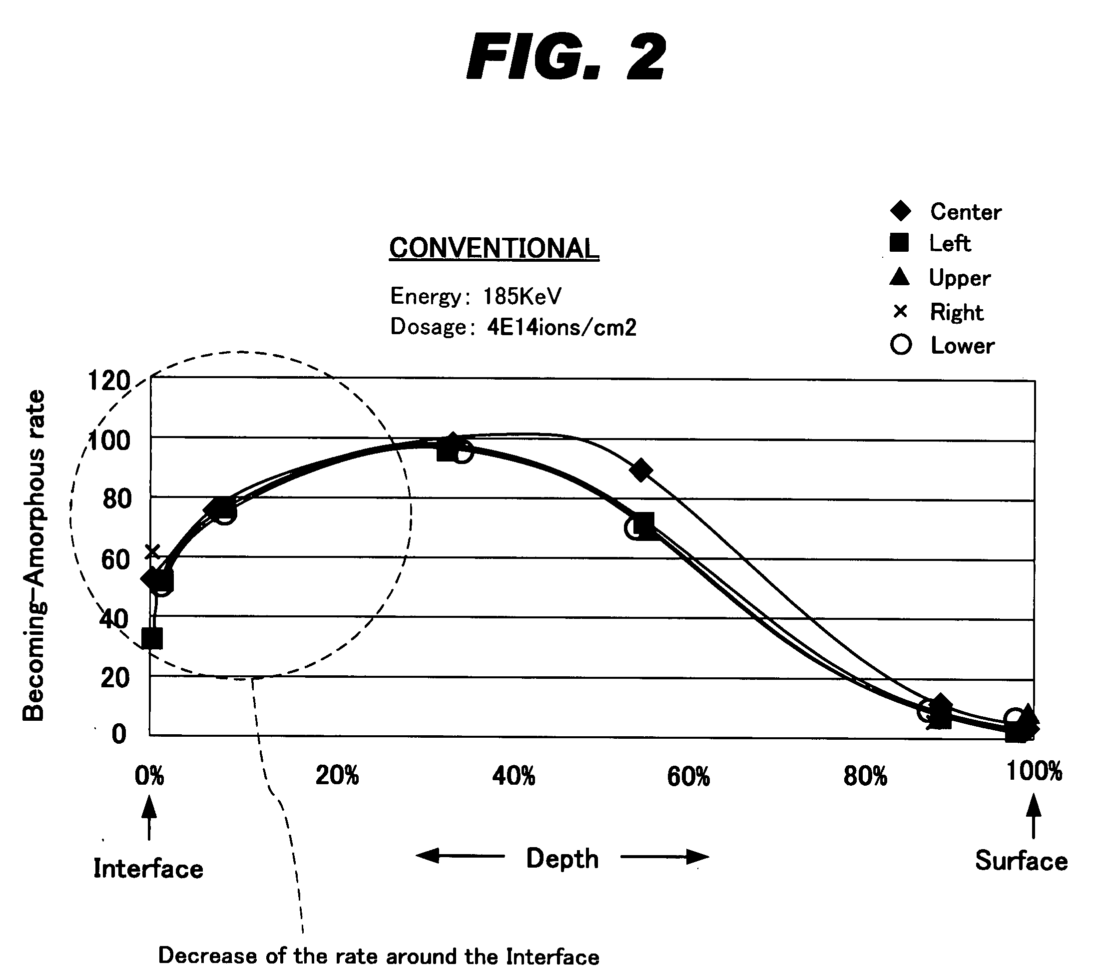
[0050]FIGS. 9 to 13 show the becoming-amorphous rate, that is, data of becoming-amorphous profile dependent upon implantation energy, of a silicon layer 12 (12b), wherein ion implantation into the silicon layer was executed under various conditions. The examples shown in FIGS. 9 and 10 employed implantation energy of 185 KeV and 170 KeV, respectively, for the conditions pertinent to comparative examples (conventional examples). The example shown in FIGS. 11, 12 and 13, to the contrary, employed implantation energy of 160 KeV, 150 KeV and 140 KeV for the condition pertinent to the presen...


PUM


Abstract

According to the present invention, a method for fabricating a semiconductor device using a Silicon-On-Sapphire (SOS) wafer comprises a process for preparing a sapphire substrate, a process for forming a silicon (Si) layer on the sapphire substrate, a process for implanting silicon ions in the silicon layer, and a process for inducing epitaxial regrowth in the silicon layer after the silicon ion implantation. The silicon ion implantation process induces the number of interstitial Si having crystalline defects in the proximity of the surface of said silicon layer to be reduced below 6.5E2/cm3; and induces an ion implantation amount per unit area of said silicon ions in the proximity of an interface between said sapphire substrate and said silicon layer to be increased to 3.0E19 ions/cm3 or more.

Description

CROSS REFERENCE TO RELATED APPLICATION[0001]This application claims the priority of Application No. 2006-263822, filed Sep. 28, 2006 in Japan, the subject matter of which is incorporated herein by reference.TECHNICAL FIELD OF THE INVENTION[0002]The present invention relates to a method for fabricating a semiconductor device using a wafer of a Silicon-On-Sapphire (SOS) structure, and, more particularly, to improved epitaxial re-growth technology for a silicon layer formed on a sapphire substrate.BACKGROUND OF THE INVENTION[0003]As described in Japanese Patent Publication No. 3492372, Silicon-On-Sapphire (SOS) wafers have been in use in high-performance MOSFET microelectronics, mainly in use for an application requiring radiation hardness. A silicon film is normally formed by epitaxial growth on a sapphire substrate. Preferably, a silicon film is thinner than a source-drain distance (channel length) and an insulating substrate is thick enough to suppress significant electrostatic coup...

Claims


Application Information

Patent Timeline
IPC IPC(8): H01L21/20
CPCH01L21/0242H01L21/02694H01L21/02532
Inventor NAGATA, TOSHIO
Owner LAPIS SEMICON CO LTD
Why Eureka
Try Eureka