Semiconductor Devices and Method of Fabricating the Same

Inactive Publication Date: 2009-05-21
DONGBU HITEK CO LTD
View PDF3 Cites 7 Cited by
  • Summary
  • Abstract
  • Description
  • Claims
  • Application Information

AI Technical Summary

Benefits of technology

[0013]As described above, according to embodiments of the invention, a contact hole with a finer width can be formed using a KrF exposure apparatus, and furthermore, contact resistance can be lowered, thereby improving device characteristics.
[0014]In addition, process margin can be realized by using a KrF exposure apparatus of low pr

Problems solved by technology

However, technical limits such as reinforcement interference of light and limits of the exposure apparatus, etc., may cause serious difficulty in forming a finer pattern such as a contact hole.
In particular, in developing products of 130 nm and 90 nm line widths using a KrF exposure apparatus, it is difficult to get a desired line width due to tight process margins.
Thus, th

Method used


Image

  • Semiconductor Devices and Method of Fabricating the Same
  • Semiconductor Devices and Method of Fabricating the Same
  • Semiconductor Devices and Method of Fabricating the Same

Examples


Embodiment Construction

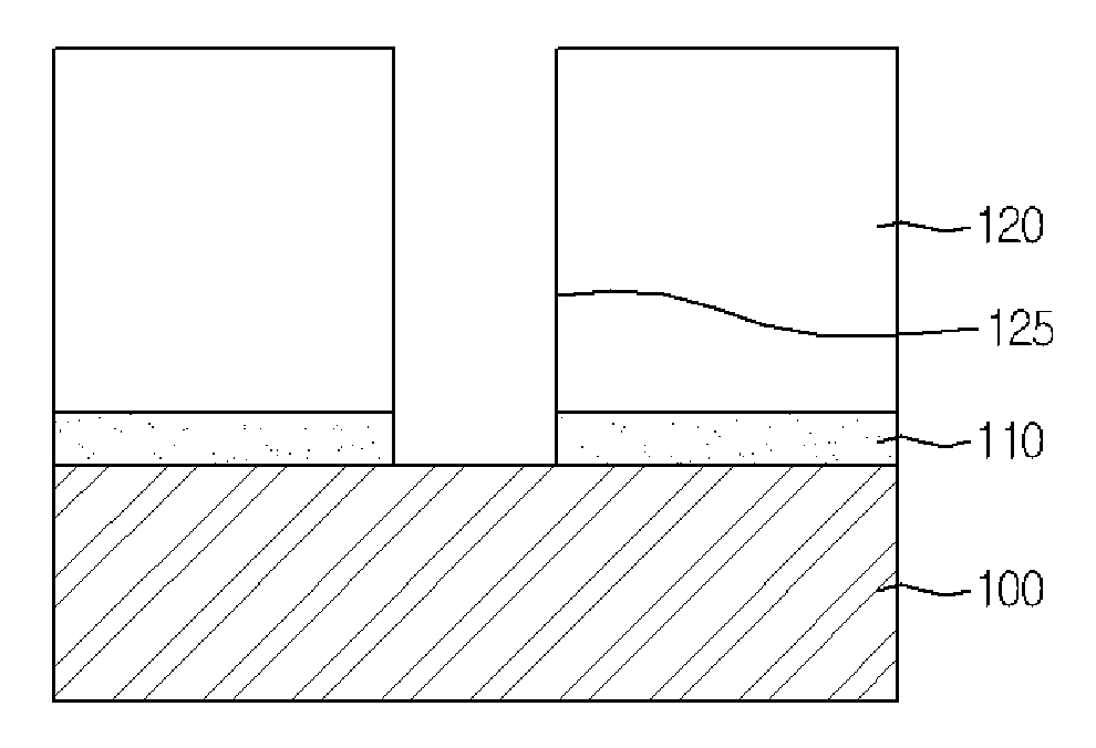
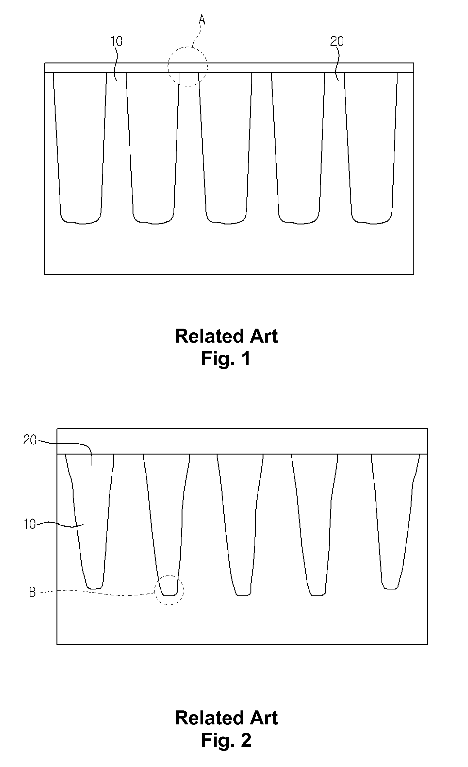
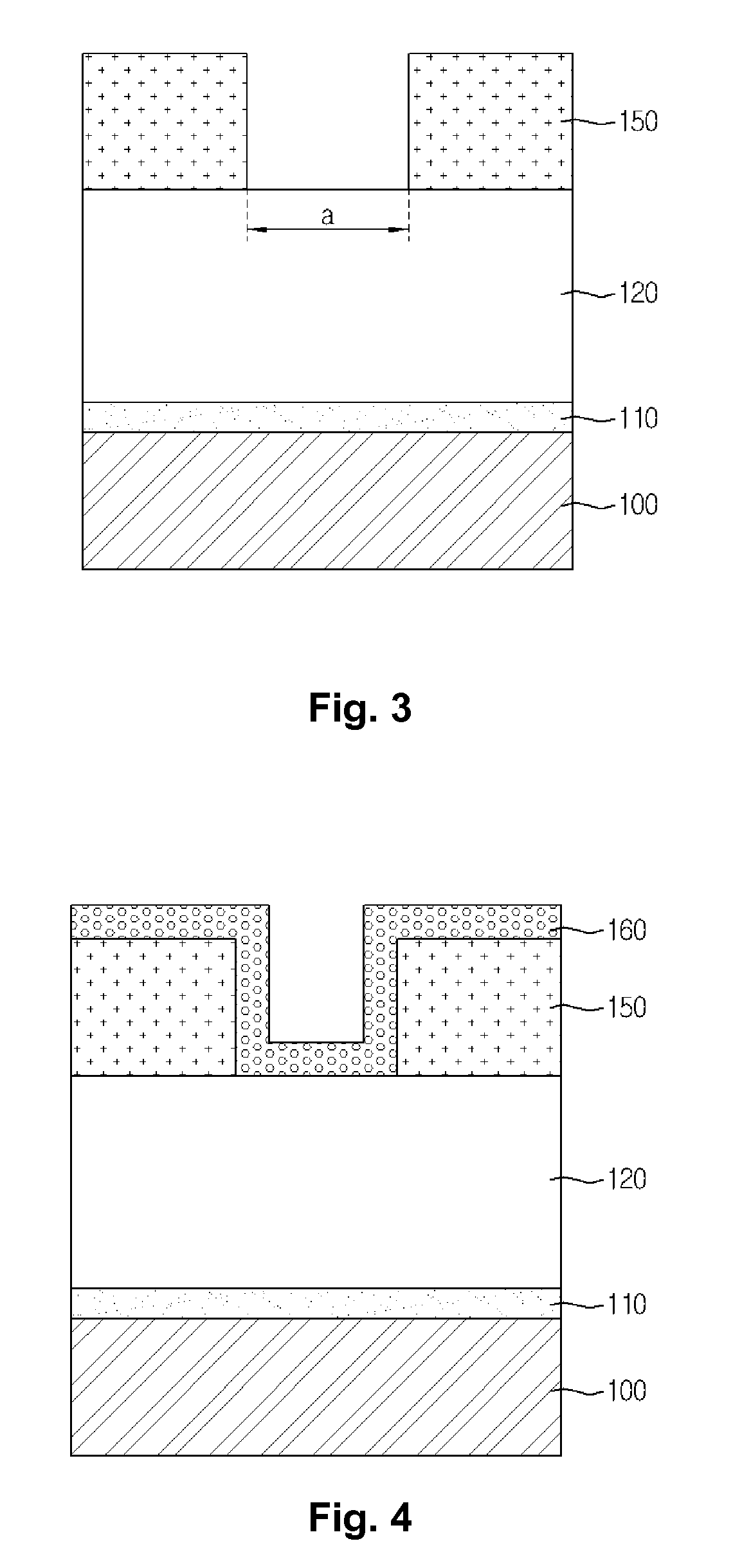
[0018]Hereinafter, a semiconductor device and a fabrication method thereof are described in detail, referring to the accompanied drawings. Components may be added, deleted or changed according to other embodiments as will be understood by those skilled in the art without deviating from the spirit of the invention.

[0019]Hereinafter, an expression to be a “first”, a “second”, etc., does not limit members, but instead, generally divides individual members of a group that includes at least two members. Therefore, it is apparent that the expression to be “first,”“second”, etc., refers to one (or more) of a plurality of members. Each member may be selectively or alternatively used. The size, measurement, of respective components in the accompanying drawings may be enlarged for facilitating an understanding of the invention. The measurement ratio of respective components described herein may be different from an actual measurement ratio. In the description, when each layer (film), an area,...


PUM


Abstract

A method of fabricating a semiconductor device is provided. A contact hole with a finer width can be formed by solving an exposure limit of KrF exposure apparatuses. The fabrication method includes forming a first insulation layer on a substrate; forming a photoresist pattern on the first insulation layer; forming a second insulation layer covering the photoresist pattern; forming a second insulation layer spacer in a sidewall of the photoresist pattern by etching the second insulation layer; forming a contact hole by etching the first insulation layer using the photoresist pattern and the second insulation layer spacer as a mask; removing the photoresist pattern; and removing the second insulation layer spacer. A contact hole with a finer width can be formed using a KrF exposure apparatus, and furthermore, contact resistance can be lowered and device characteristics can be improved

Description

[0001]The present application claims priority under 35 U.S.C. 119 and 35 U.S.C. 365 to Korean Patent Application No. 10-2007-0117288 (filed on Nov. 16, 2007), which is hereby incorporated by reference in its entirety.BACKGROUNDDescription of the Related Art[0002]A photolithography process is a necessary process in fabricating semiconductor devices. The process generally involves evenly covering a photoresist layer on a wafer, performing an exposure process using a photo mask corresponds to a given layout, and developing an exposed photoresist layer to form the photoresist layer in a pattern of specific shape.[0003]Semiconductor photolithography technology used in the photolithography process performed in fabricating the semiconductor device provides a precise mask design. Accordingly the amount of light projected through the mask can be appropriately controlled.[0004]An increasingly higher integration tendency of recent semiconductor devices uses more detailed and finer design rules...

Claims


Application Information

Patent Timeline
IPC IPC(8): H01L21/311
CPCH01L21/0337H01L21/0338H01L21/31144H01L21/76816G03F7/168G03F7/38
Inventor LEE, KANG HYUN
Owner DONGBU HITEK CO LTD
Why Eureka
Try Eureka