Oxide semiconductor thin film transistor and method of forming the same

a thin film transistor and oxide semiconductor technology, applied in the direction of transistors, semiconductor devices, electrical devices, etc., can solve the problems of deterioration of the performance of the oxide semiconductor thin film transistor and the length of the effective channel in the semiconductor layer, so as to reduce the introduction of hydrogen, improve device characteristics, and minimize the effect of introduction of hydrogen

Pending Publication Date: 2021-10-07
LG DISPLAY CO LTD
View PDF9 Cites 2 Cited by
  • Summary
  • Abstract
  • Description
  • Claims
  • Application Information

AI Technical Summary

Benefits of technology

[0014]An object of the present disclosure is to provide an oxide semiconductor thin film transistor capable of minimizing the introduction of hydrogen into the oxide semiconductor and improving the device characteristics.
[0015]Generally, the length of an effective channel in the semiconductor layer formed of an oxide semiconductor in the related art can be decreased by diffusing the impurities generated inside the display device during the formation process into the oxide semiconductor, and the performance of the oxide semiconductor thin film transistor can be

Problems solved by technology

Generally, the length of an effective channel in the semiconductor layer formed of an oxide semiconductor in the related art can be decreased by diffusing the impurities genera

Method used


Image

  • Oxide semiconductor thin film transistor and method of forming the same
  • Oxide semiconductor thin film transistor and method of forming the same
  • Oxide semiconductor thin film transistor and method of forming the same

Examples


Embodiment Construction

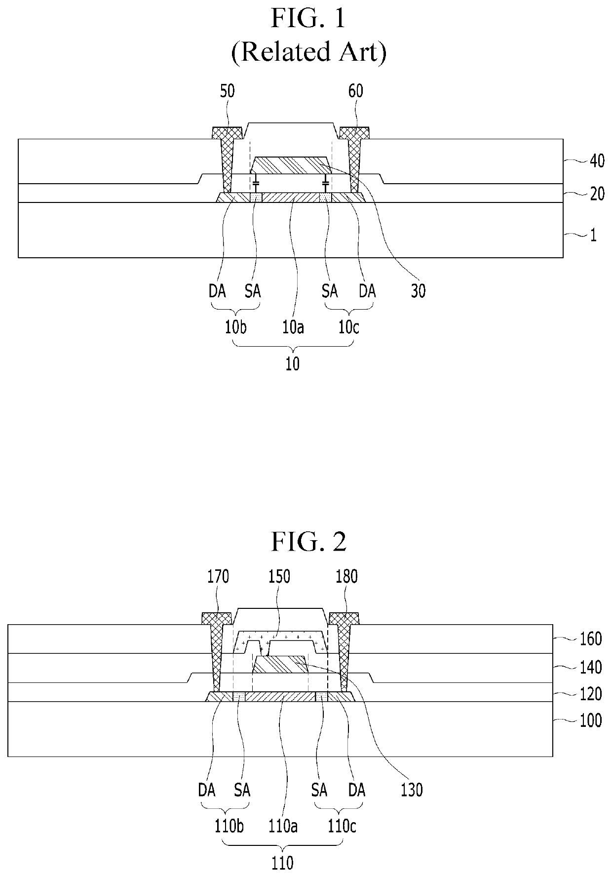
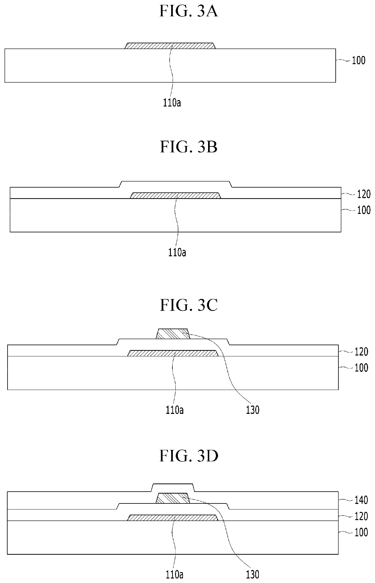
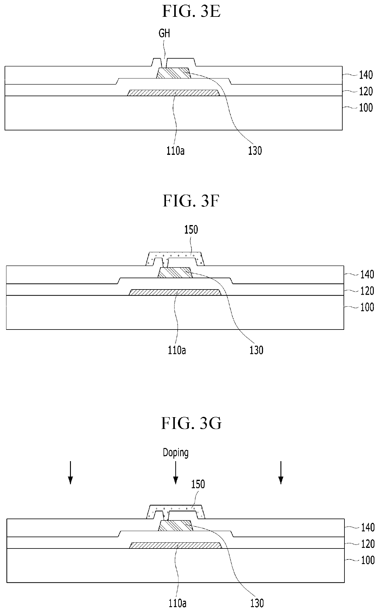
[0025]Reference will now be made in detail to the preferred embodiments of the present disclosure, examples of which are illustrated in the accompanying drawings. Wherever possible, the same reference numbers will be used throughout the drawings to refer to the same or like parts.

[0026]The advantages and features of the present disclosure and methods of achieving the same will be more clearly understood from the following detailed description taken in conjunction with the accompanying drawings. However, the present disclosure is not limited to the embodiments described below, and can be implemented in various forms. The embodiments of the present disclosure are provided only to completely disclose the present disclosure and fully inform a person having ordinary knowledge in the field to which the present disclosure pertains of the scope of the present disclosure. Accordingly, the present disclosure is defined only by the scope of the claims.

[0027]The shapes, sizes, ratios, angles, n...


PUM


Abstract

An oxide semiconductor thin film transistor and a method of forming the oxide semiconductor thin film transistor are provided. The oxide semiconductor thin film transistor can include a semiconductor layer including a channel region, a source region and a drain region; a first gate insulating layer on the semiconductor layer; a gate electrode on the first gate insulating layer; a second gate insulating layer on the gate electrode; an auxiliary electrode on the second gate insulating layer; an interlayer insulating layer on the auxiliary electrode; and a source electrode and a drain electrode on the interlayer insulating layer, wherein the source region and the drain region being disposed at both sides of the channel region, wherein the gate electrode overlapping with the channel region, and the auxiliary electrode overlapping with the gate electrode.

Description

CROSS-REFERENCE TO RELATED APPLICATIONS[0001]This application claims the priority benefit of the Korean Patent Application No. 10-2020-0040142 filed on Apr. 2, 2020 in the Republic of Korea, the entire contents of which are hereby expressly incorporated by reference as if fully set forth herein into the present application.BACKGROUND OF THE INVENTIONField of the Invention[0002]The present disclosure relates to an oxide semiconductor thin film transistor capable of improving a device characteristic of a thin film transistor, and a method of forming the same.Discussion of the Related Art[0003]Recently, a flat panel display device, such as a liquid crystal display device and an organic light emitting diode display device, have been developed. Further, research on a display device having a large size and high resolution is actively progressing. Thus, the development of a thin film transistor for securing stable operation and reliability of the display device is needed.[0004]In the displ...

Claims


Application Information

Patent Timeline
IPC IPC(8): H01L29/786H01L29/66
CPCH01L29/7869H01L29/66742H01L29/78696H01L29/78618H01L29/42384H01L29/78645H01L29/41733H01L29/458H01L29/66969
Inventor JI, HYUKJEON, JIN CHAEKIMCHOI, SUN YOUNGJEONG, MI JIN
Owner LG DISPLAY CO LTD
Why Eureka
Try Eureka