Method of forming multi-layers for a thin film transistor

a thin film transistor and multi-layer technology, applied in the field of thin film transistors, can solve the problems of unacceptably high water content degrading the performance of tfts, process complicating the fabrication of tfts, and formed silicon dioxide, so as to improve the device characteristics of tfts, simplify the tft fabrication process, and reduce water or hydrogen content

Inactive Publication Date: 2005-05-31
SHARP LAB OF AMERICA INC
View PDF7 Cites 2 Cited by
  • Summary
  • Abstract
  • Description
  • Claims
  • Application Information

AI Technical Summary

Benefits of technology

[0012]The present invention has advantages such as simplifying the TFT fabrication process while improving the...

Problems solved by technology

Unfortunately, the silicon dioxide formed in accordance with such conventional methods often has an unacceptably high water content degrading the performance of the TFTs.
However, such extra annealing processes complicate the fabrication of the TFTs and become a source of contamination.
This is because, while the glass substrate is annealed and carried between annealing furnaces and deposition chambers, the surface of the ...

Method used


Image

  • Method of forming multi-layers for a thin film transistor
  • Method of forming multi-layers for a thin film transistor
  • Method of forming multi-layers for a thin film transistor

Examples


Embodiment Construction

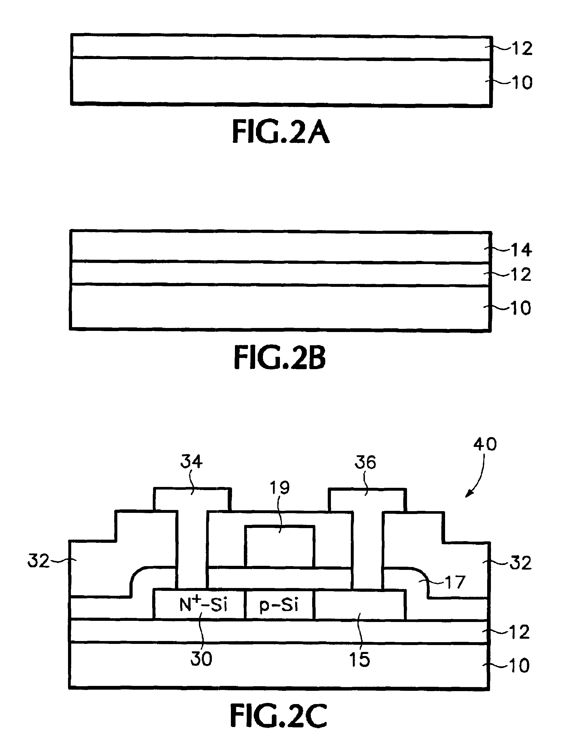
[0020]In the following description, numerous specific details are set forth to provide a thorough understanding of the present invention. However, one having ordinary skill in the art should recognize that the invention can be practiced without these specific details. In some instances, well-known process steps, device structures, and techniques have not been shown in detail to avoid obscuring the present invention.

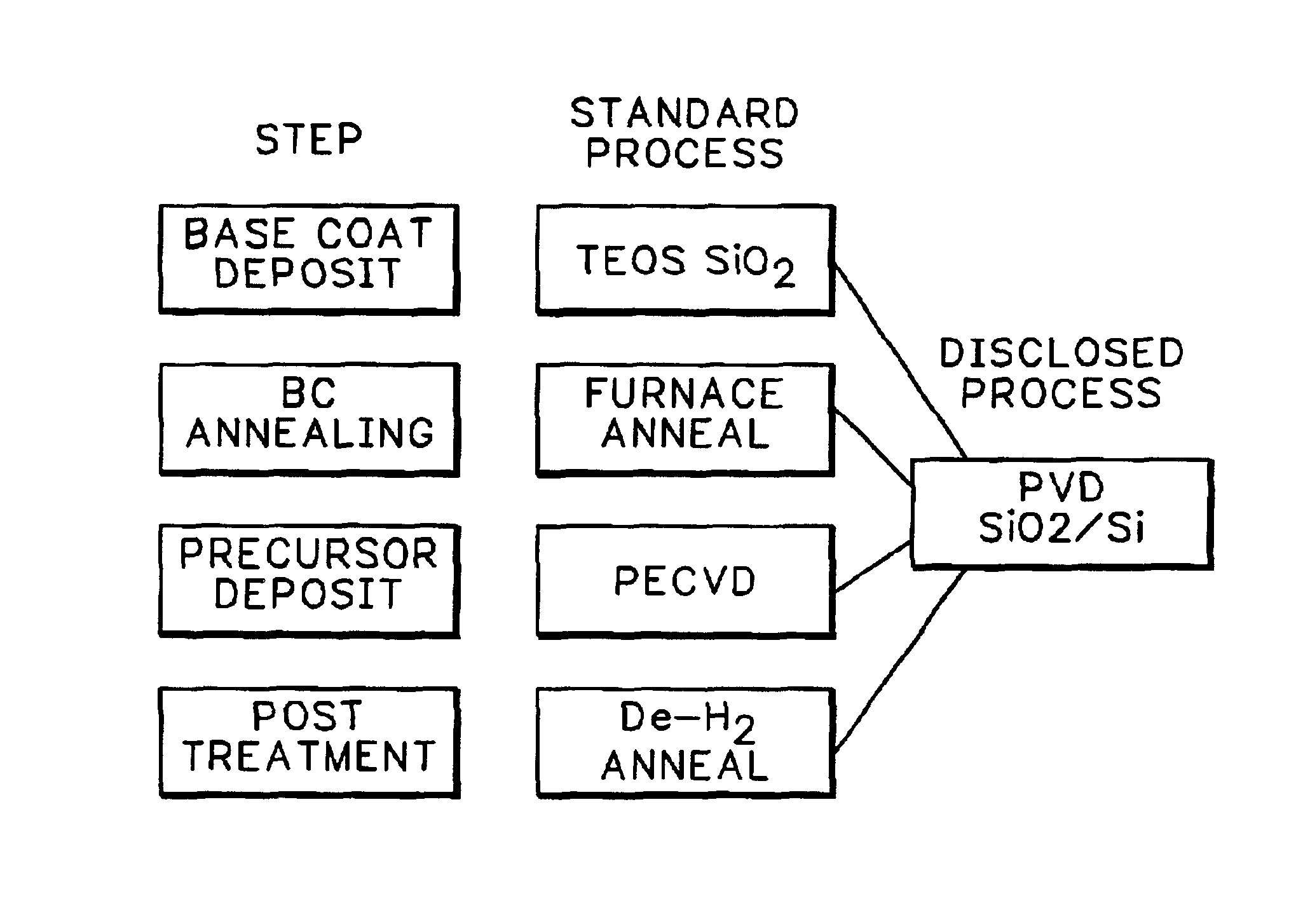
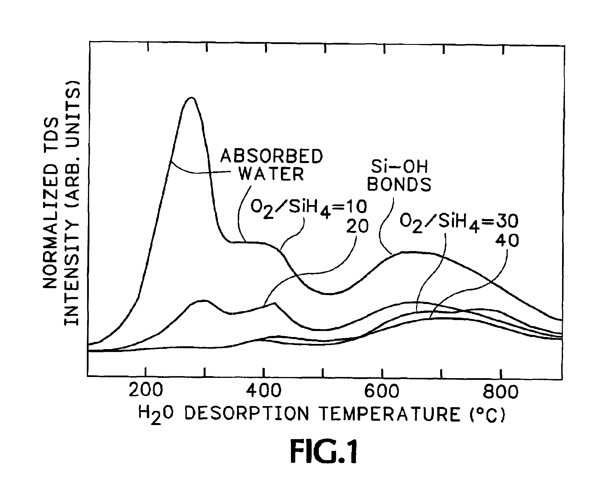
[0021]The inventors of the present invention have determined that the sources of water contained in a silicon dioxide base-coat (BC) layer can be manifested in two main ways: (1) the water content resulting from Si—OH bonds in the silicon dioxide layer, (2) the water content resulting from absorbed water in the silicon dioxide layer upon exposure to an ambient.

[0022]The first source can be attributed to the deposition chemistry, i.e. interaction of H, O and Si as the layer is formed from precursors such as SiH4 or tetraethylorthosilicate (TEOS). The second source depends ...


PUM


Abstract

The present invention concerns a method of forming multi-layers such as base-coat and active layers for TFTs. In accordance with the preferred embodiment of the present invention, a first layer is formed on a transparent substrate using a physical vapor deposition. And a second layer is sequentially formed using a physical vapor deposition on the first layer without breaking vacuum.
The present invention simplifies the TFT fabrication while decreasing the water or hydrogen content within multilayers including a base-coat (BC) layer.

Description

BACKGROUND OF THE INVENTION[0001]1. The Field of the Invention[0002]This invention relates generally to the field of thin film transistors (TFT), and more particularly, to a method of forming a number of thin-layer materials used in the fabrication of thin-film-transistors (TFTs) for devices such as a liquid crystal display (LCD).[0003]2. Description of the Related Art[0004]In the manufacture of thin film transistor (TFT) liquid-crystal-displays (LCDs), the active region of the display consists of an array of pixels, built on a glass substrate. The TFTs are made by various typical semiconductor processes on the glass substrate.[0005]Before fabricating the TFTs, in general, the glass substrate needs to be coated with a base-coat (BC) layer to prevent outdiffusion of impurities, typically present in the glass material, to the TFT layers. The most typical base-coat material is silicon dioxide that is deposited by conventional CVD (chemical vapor deposition) processes.[0006]Unfortunatel...

Claims


Application Information

Patent Timeline
IPC IPC(8): H01L21/02H01L21/336H01L29/66H01L29/786G02F1/1368G02F1/13H01L21/316
CPCH01L29/78606H01L29/66757
Inventor VOUTSAS, APOSTOLOSNAKATA, YUKIHIKO
Owner SHARP LAB OF AMERICA INC
Why Eureka
Try Eureka