Semiconductor device and method for manufacturing the same

a semiconductor memory and semiconductor technology, applied in the direction of semiconductor devices, electrical devices, transistors, etc., can solve the problems of increasing the leakage current of the structure, the active region may not be opened, and the overall area of the complicated semiconductor memory apparatus is difficult to reduce, so as to increase the process margin and improve the device characteristics

Active Publication Date: 2015-09-01
SK HYNIX INC
View PDF3 Cites 1 Cited by
  • Summary
  • Abstract
  • Description
  • Claims
  • Application Information

AI Technical Summary

Benefits of technology

[0010]An embodiment of the present invention relates to a semiconductor device for improving device characteristics by increasing a process margin between an active region and a storage node contact.

Problems solved by technology

Reducing the overall area of a complicated semiconductor memory apparatus is difficult due to the plurality of transistors contained in the semiconductor device.
However, the isolation gate structure increases a leakage current in a cell area more than a trench-type device isolation film.
In addition, when etching a contact hole in an active region in a subsequent etch process, the active region may not be opened.
If the contact hole size is increased to prevent the above-mentioned problems, short-circuiting may occur between the contact hole and the storage node.
The storage node contact must be formed by a Self Aligned Contact (SAC) process after bit-line formation, and contact resistance unavoidably increases as a contact area between the active region and the contact is reduced.

Method used


Image

  • Semiconductor device and method for manufacturing the same
  • Semiconductor device and method for manufacturing the same
  • Semiconductor device and method for manufacturing the same

Examples


Embodiment Construction

[0033]Reference will now be made in detail to embodiments of the present invention, examples of which are illustrated in the accompanying drawings. Wherever possible, the same reference numbers will be used throughout the drawings to refer to the same or like parts. A semiconductor device and a method for manufacturing the same according to embodiments of the present invention will hereinafter be described with reference to the accompanying drawings.

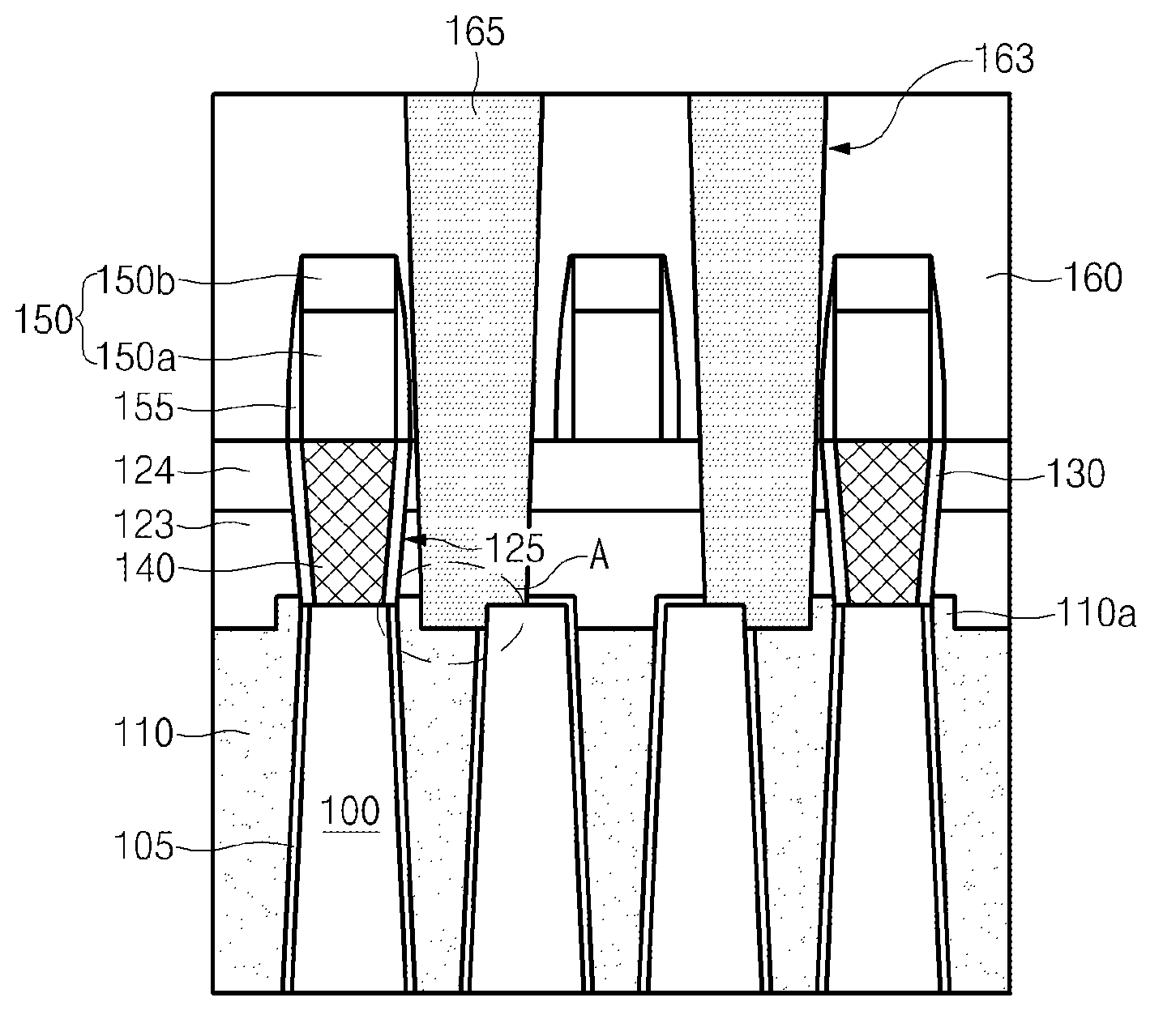
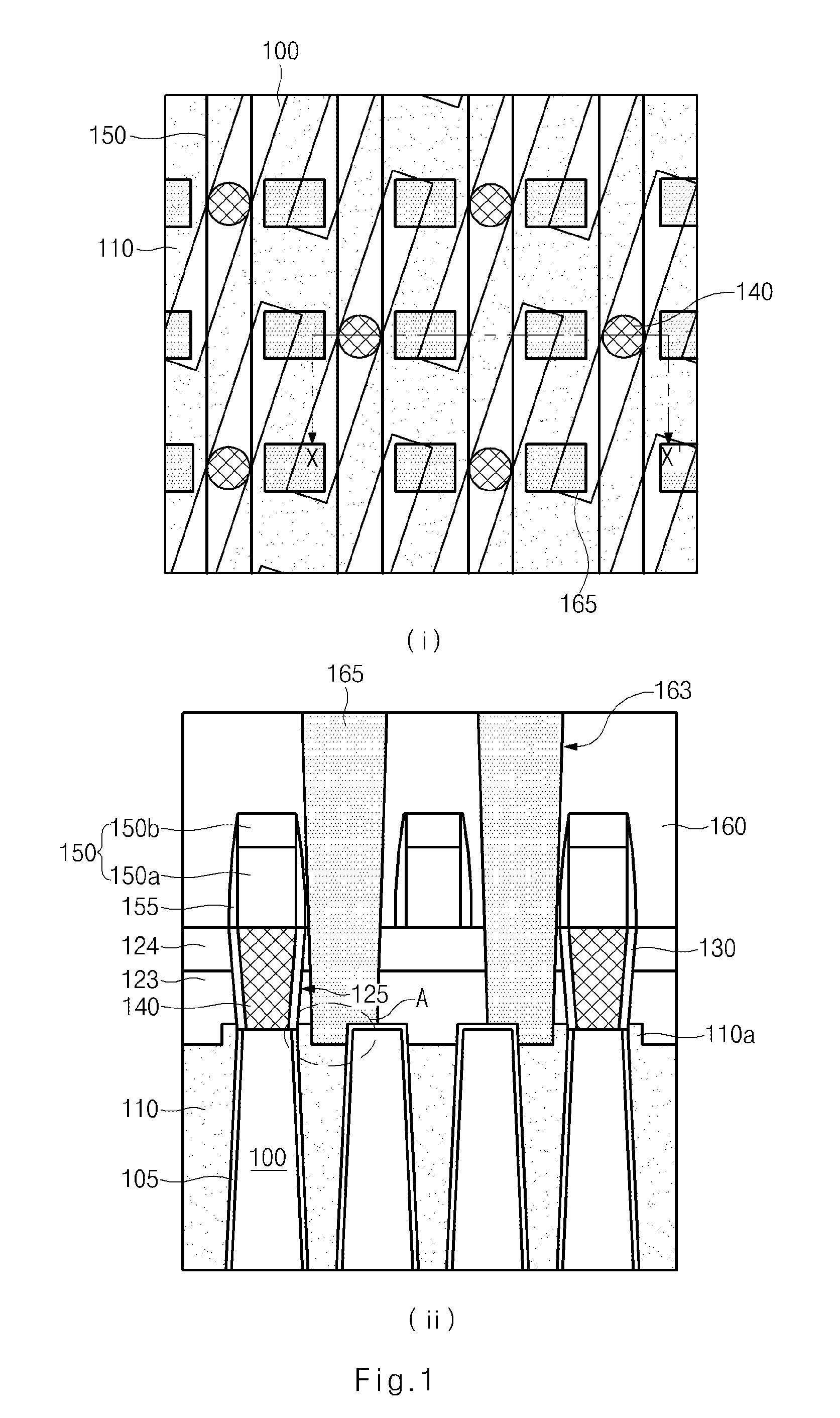
[0034]FIG. 1 shows a plan view and a cross-sectional view illustrating a semiconductor device according to an embodiment of the present invention. In more detail, FIG. 1(ii) is a cross-sectional view illustrating the semiconductor device taken along the line X-X′ of FIG. 1(i).

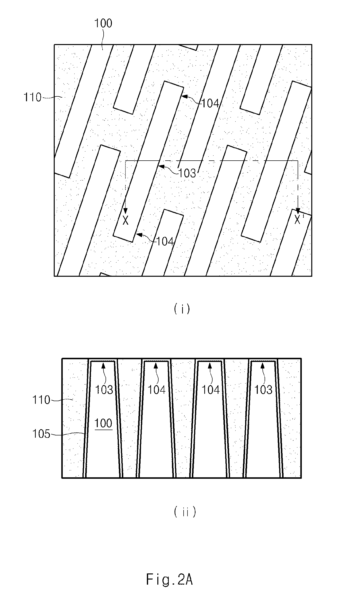
[0035]Referring to FIG. 1, an active region 100 and a device isolation film 110 are formed over a semiconductor substrate. As illustrated in FIG. 2A, the active region 100 is formed as a bar type, and the active region 100 includes a bit line contact region 103 and ...


PUM


Abstract

A semiconductor device and a method for manufacturing the same are disclosed, which can improve device characteristics by increasing a process margin between an active region and a storage node contact. The semiconductor device includes an active region, a device isolation film formed to have a lower height than the active region, and exposing an upper part of the active region, and a barrier pattern formed at a sidewall of the exposed active region of an upper part of the device isolation film.

Description

CROSS-REFERENCE TO RELATED APPLICATION[0001]The priority of Korean patent application No. 10-2011-0141359 filed on 23 Dec. 2011, the disclosure of which is hereby incorporated in its entirety by reference, is claimed.BACKGROUND OF THE INVENTION[0002]Embodiments of the present invention relate to a semiconductor device and a method for manufacturing the same, and more particularly to a semiconductor device including a buried gate, a storage node and a bit line, and a method for manufacturing the same.[0003]A Dynamic Random Access Memory (DRAM) includes a plurality of unit cells, each of which includes a capacitor and a transistor. The capacitor is used to temporarily store data therein. The transistor is used to transmit data between a bit line and the capacitor in correspondence with a control signal (i.e., a word line) using the electric conductivity of a semiconductor material, which changes depending on environment. The transistor has three regions including a gate, a source and ...

Claims


Application Information

Patent Timeline
Patent Type & Authority Patents(United States)
IPC IPC(8): H01L27/108H01L21/768
CPCH01L27/10855H01L21/76897H01L27/10814H01L27/10876H10B12/0335H01L21/28H10B99/00H10B12/00H10B12/053H10B12/315
Inventor LEE, SEONG EUN
Owner SK HYNIX INC
Why Eureka
Try Eureka